This document provides information on the Central Semiconductor D41D series PNP silicon power transistors. It includes a description of the transistors and their intended applications in amplification and switching. It also lists the full part numbers, maximum ratings, electrical characteristics, lead configuration, and manufacturer contact information for technical support.
1. D41D1 D41D7 D41D13
D41D2 D41D8 D41D14
D41D4 D41D10
D41D5 D41D11
PNP SILICON
POWER TRANSISTORS
DESCRIPTION:
The CENTRAL SEMICONDUCTOR D41D series types
are PNP silicon power transistors designed for amplifier
and switching applications. The NPN complementary
types are the D40D series.
MARKING: FULL PART NUMBER
D41D10
D41D11
D41D1 D41D4 D41D7 D41D13
MAXIMUM RATINGS: (TC=25°C) SYMBOL D41D2 D41D5 D41D8 D41D14 UNITS
Collector-Emitter Voltage VCES 45 60 75 90 V
Collector-Emitter Voltage VCEO 30 45 60 75 V
Emitter-Base Voltage VEBO 5.0 V
Continuous Collector Current IC 1.0 A
Peak Collector Current ICM 1.5 A
Power Dissipation PD 6.25 W
Operating and Storage Junction Temperature TJ, Tstg -65 to +150 °C
Thermal Resistance ΘJC 20 °C/W
ELECTRICAL CHARACTERISTICS: (TC=25°C unless otherwise noted)
SYMBOL TEST CONDITIONS MIN MAX UNITS
ICES VCE=Rated VCES 100 nA
IEBO VEB=5.0V 100 nA
BVCEO lC=10mA (D41D1, 2) 30 V
BVCEO lC=10mA (D41D4, 5) 45 V
BVCEO lC=10mA (D41D7, 8) 60 V
BVCEO lC=10mA (D41D10, 11, 13, 14) 75 V
VCE(SAT) lC=500mA, IB=50mA (D41D1, 2, 4, 5) 0.5 V
VCE(SAT) lC=500mA, IB=50mA (D41D7, 8, 10, 11, 13, 14) 1.0 V
VBE(SAT) lC=500mA, IB=50mA 1.5 V
D41D1
D41D4 D41D5
D41D7 D41D8
D41D10 D41D11
D41D13 D41D2 D41D14
MIN MAX MIN MAX MIN MAX
hFE VCE=2.0V, IC=100mA 50 150 120 300 120 360
hFE VCE=2.0V, IC=1.0A
(Except D41D13, 14) 10 - 20 - 10 -
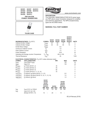
TO-202 CASE
R2 (4-February 2016)
www.centralsemi.com
2. D41D1 D41D7 D41D13
D41D2 D41D8 D41D14
D41D4 D41D10
D41D5 D41D11
PNP SILICON
POWER TRANSISTORS
LEAD CODE:
1) Emitter
2) Base
3) Collector
Tab is common to pin 3
MARKING:
FULL PART NUMBER
TO-202 CASE - MECHANICAL OUTLINE
www.centralsemi.com
R2 (4-February 2016)
3. For the latest version of Central Semiconductor’s LIMITATIONS AND DAMAGES DISCLAIMER,
which is part of Central’s Standard Terms and Conditions of sale, visit: www.centralsemi.com/terms
OUTSTANDING SUPPORT AND SUPERIOR SERVICES
PRODUCT SUPPORT
Central’s operations team provides the highest level of support to insure product is delivered on-time.
• Supply management (Customer portals) • Custom bar coding for shipments
• Inventory bonding • Custom product packing
• Consolidated shipping options
CONTACT US
Corporate Headquarters & Customer Support Team
Central Semiconductor Corp.
145 Adams Avenue
Hauppauge, NY 11788 USA
Main Tel: (631) 435-1110
Main Fax: (631) 435-1824
Support Team Fax: (631) 435-3388
www.centralsemi.com
Worldwide Field Representatives:
www.centralsemi.com/wwreps
Worldwide Distributors:
www.centralsemi.com/wwdistributors
DESIGNER SUPPORT/SERVICES
Central’s applications engineering team is ready to discuss your design challenges. Just ask.
• Free quick ship samples (2nd day air) • Special wafer diffusions
• Online technical data and parametric search • PbSn plating options
• SPICE models • Package details
• Custom electrical curves • Application notes
• Environmental regulation compliance • Application and design sample kits
• Customer specific screening • Custom product and package development
• Up-screening capabilities
(001)
REQUESTING PRODUCT PLATING
1. If requesting Tin/Lead plated devices, add the suffix “ TIN/LEAD” to the part number when
ordering (example: 2N2222A TIN/LEAD).
2. If requesting Lead (Pb) Free plated devices, add the suffix “ PBFREE” to the part number
when ordering (example: 2N2222A PBFREE).
www.centralsemi.com