Design Note – DN06054/D
Reference Design
for Solar Power MPPT Controller
Device Application Input
Voltage
Output
Voltage
Output
Current
Topology
NCP1294 Solar Street Lighting 12-24 V A 13.2V A 2.0A Flyback
Table 1: NCP1294 Output Statistics
Characteristic Min Typ Max Unit
Output Voltage 9 12 13.5 V
Output Current 0 2.0 A
Oscillator Frequency 100 kHz
1. < 2mA Current Consumption from Battery
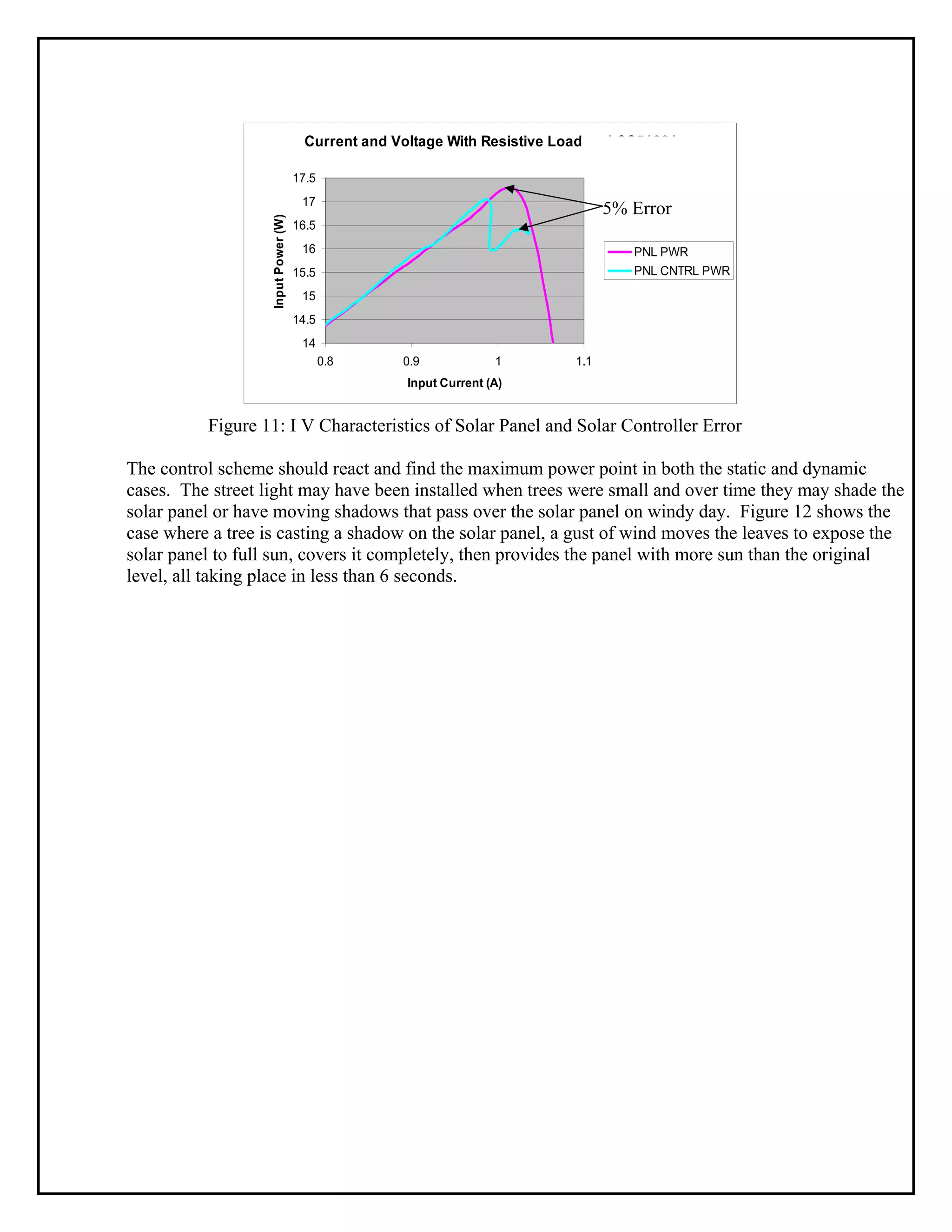
2. Maximum Power Tracking < 5% Error
3. Can Charge 4 Batteries in Series or Parallel
4. Can be Configured for use with 10W to 30W Solar Panels
5. Can be used in Parallel with Other Systems
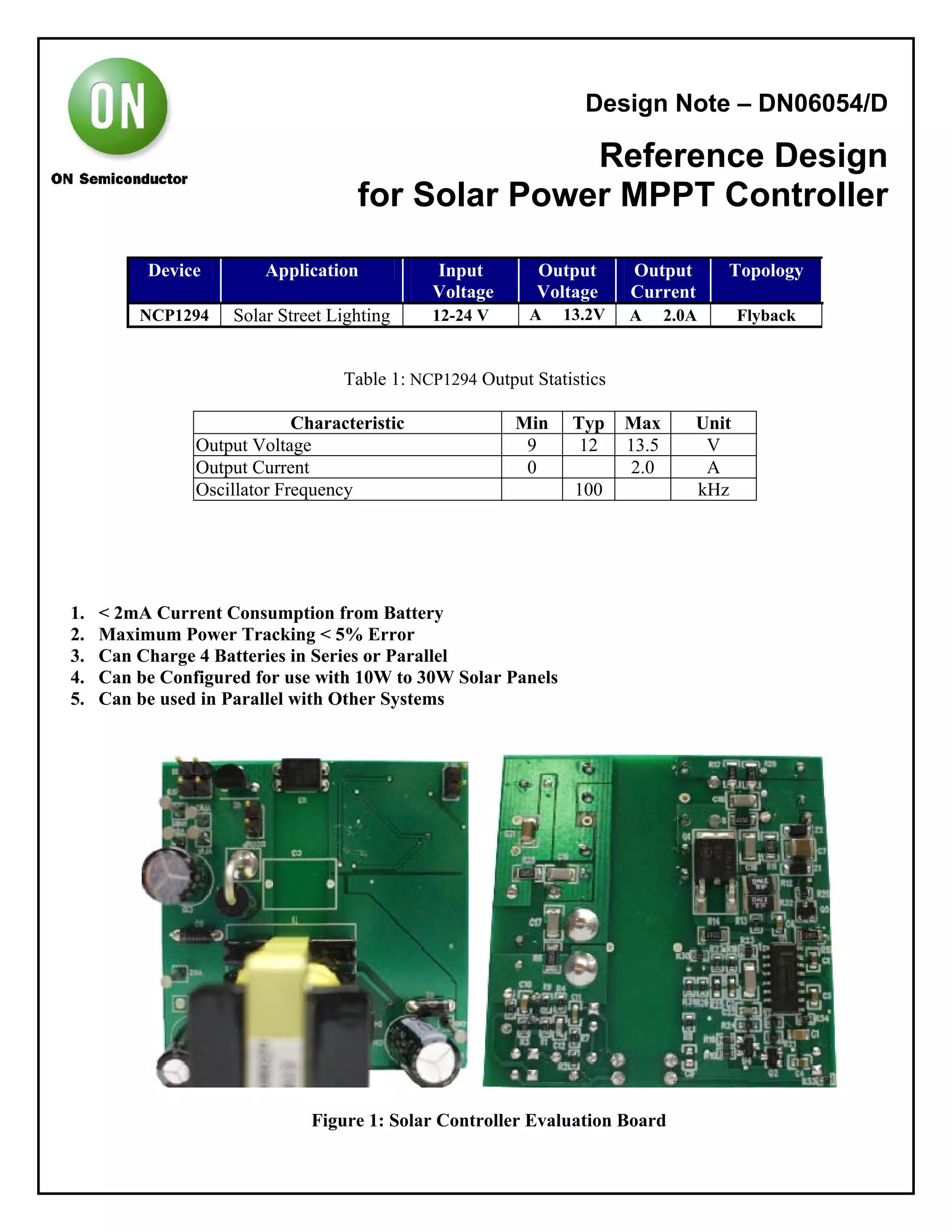
Figure 1: Solar Controller Evaluation Board
System Description
The system under consideration is an off grid solar streetlamp. The solar streetlamp consists of high power LEDS,
a lead acid battery, a solar controller, and a solar panel as shown in Figure 2.
Solar
Controller
12V+
-
Solar
Panel
Solar
Controller
Lead Acid
Battery
LED
Street
Light
Figure 2: Basic off Grid Solar Streetlamp System
Solar Panel Characteristics
Solar panels collect energy from the sun and convert it to electrical energy. Unfortunately, the sun is not consistent
throughout the day due to cloud cover and the angle of the sun relative to the position of the solar panel. Further,
the intensity of the sun varies with the season, geographic location, and reflections from adjacent surfaces. Figure 3
shows the monthly average daily total solar resource information on grid cells of approximately 40 km by 40 km in
size [1].
Figure 3: Monthly Average Daily Total Solar Resource in December (Right) and July (Left) [1]
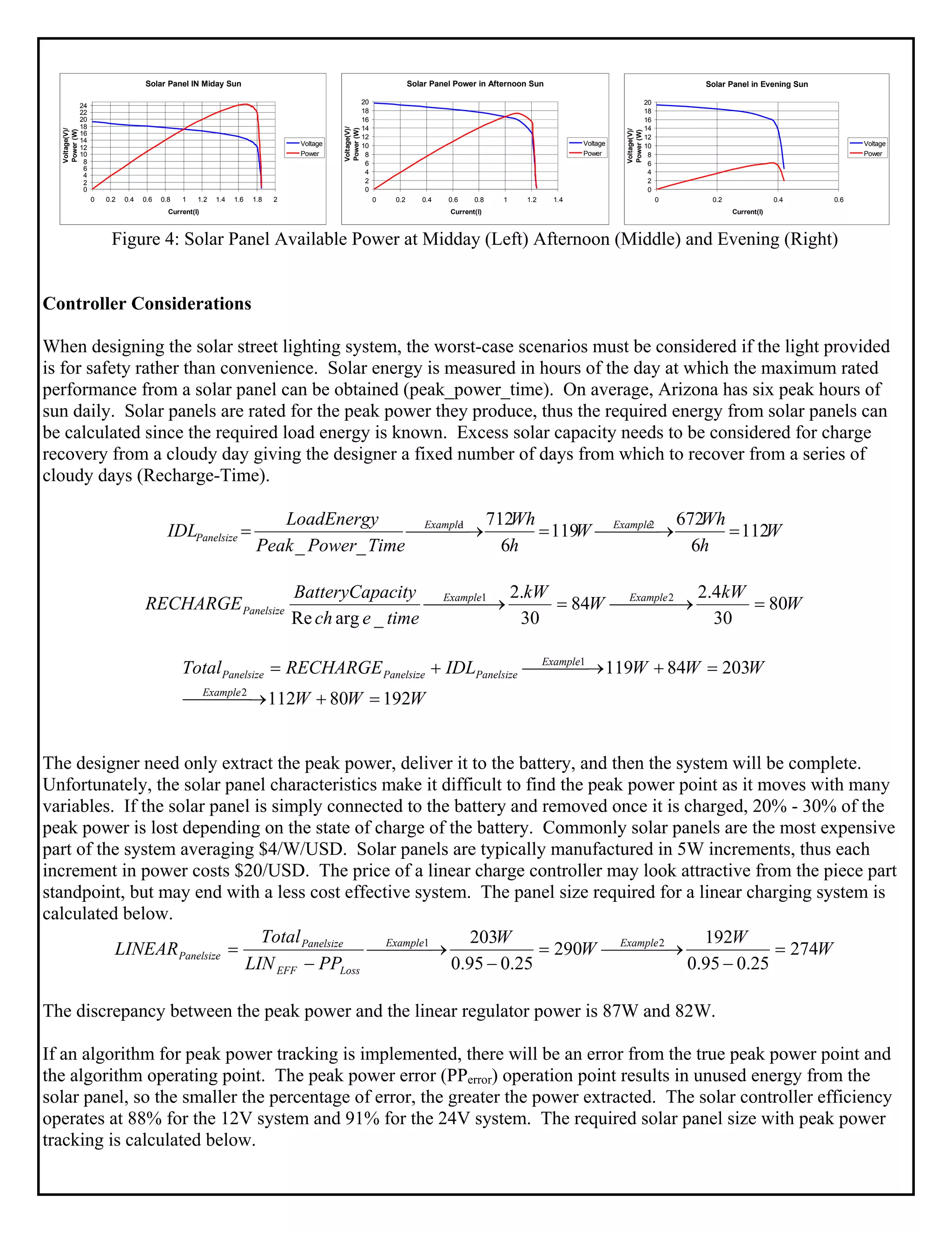
Since the sun is not consistent, the solar panel rated for 30W peak power may only supply 24W in midday sun and
6 W in the evening sun. Figure 4 displays the voltage, current, and power characteristics of a solar panel at various
times during the day with a resistive load. The voltage from solar panels can be configured by the manufacturer to
supply almost any voltage and current depending on the solar cell configuration, but generally range from 20V to
48V.
Solar Panel IN Miday Sun
0
2
4
6
8
10
12
14
16
18
20
22
24
0 0.2 0.4 0.6 0.8 1 1.2 1.4 1.6 1.8 2
Current(I)
Voltage(V)/
Power(W)
Voltage
Power
Solar Panel Power in Afternoon Sun
0
2
4
6
8
10
12
14
16
18
20
0 0.2 0.4 0.6 0.8 1 1.2 1.4
Current(I)
Voltage(V)/
Power(W)
Voltage
Power
Solar Panel in Evening Sun
0
2
4
6
8
10
12
14
16
18
20
0 0.2 0.4 0.6
Current(I)
Voltage(V)/
Power(W)
Voltage
Power
Figure 4: Solar Panel Available Power at Midday (Left) Afternoon (Middle) and Evening (Right)
Controller Considerations
When designing the solar street lighting system, the worst-case scenarios must be considered if the light provided
is for safety rather than convenience. Solar energy is measured in hours of the day at which the maximum rated
performance from a solar panel can be obtained (peak_power_time). On average, Arizona has six peak hours of
sun daily. Solar panels are rated for the peak power they produce, thus the required energy from solar panels can
be calculated since the required load energy is known. Excess solar capacity needs to be considered for charge
recovery from a cloudy day giving the designer a fixed number of days from which to recover from a series of
cloudy days (Recharge-Time).
W
h
Wh
W
h
Wh
TimePowerPeak
LoadEnergy
IDL ExampleExample
Panelsize 112
6
672
119
6
712
__
21
=⎯⎯⎯ →⎯=⎯⎯⎯ →⎯=
W
kW
W
kW
timeech
acityBatteryCap
RECHARGE ExampleExample
Panelsize 80
30
4.2
84
30
.2
_argRe
21
=⎯⎯⎯ →⎯=⎯⎯⎯ →⎯
WWW
WWWIDLRECHARGETotal
Example
Example
PanelsizePanelsizePanelsize
19280112
20384119
2
1
=+⎯⎯⎯ →⎯
=+⎯⎯⎯ →⎯+=
The designer need only extract the peak power, deliver it to the battery, and then the system will be complete.
Unfortunately, the solar panel characteristics make it difficult to find the peak power point as it moves with many
variables. If the solar panel is simply connected to the battery and removed once it is charged, 20% - 30% of the
peak power is lost depending on the state of charge of the battery. Commonly solar panels are the most expensive
part of the system averaging $4/W/USD. Solar panels are typically manufactured in 5W increments, thus each
increment in power costs $20/USD. The price of a linear charge controller may look attractive from the piece part
standpoint, but may end with a less cost effective system. The panel size required for a linear charging system is
calculated below.
W
W
W
W
PPLIN
Total
LINEAR ExampleExample
LossEFF
Panelsize
Panelsize 274
25.095.0
192
290
25.095.0
203 21
=
−
⎯⎯⎯ →⎯=
−
⎯⎯⎯ →⎯
−
=
The discrepancy between the peak power and the linear regulator power is 87W and 82W.
If an algorithm for peak power tracking is implemented, there will be an error from the true peak power point and
the algorithm operating point. The peak power error (PPerror) operation point results in unused energy from the
solar panel, so the smaller the percentage of error, the greater the power extracted. The solar controller efficiency
operates at 88% for the 12V system and 91% for the 24V system. The required solar panel size with peak power
tracking is calculated below.
WW
W
PP
IDL
MPT ExampleExample
ERROR
Panelsize
Panelsize 223
%5%91
192
254
%5%85
203 21
=
−
⎯⎯⎯ →⎯=
−
⎯⎯⎯ →⎯
−
=
η
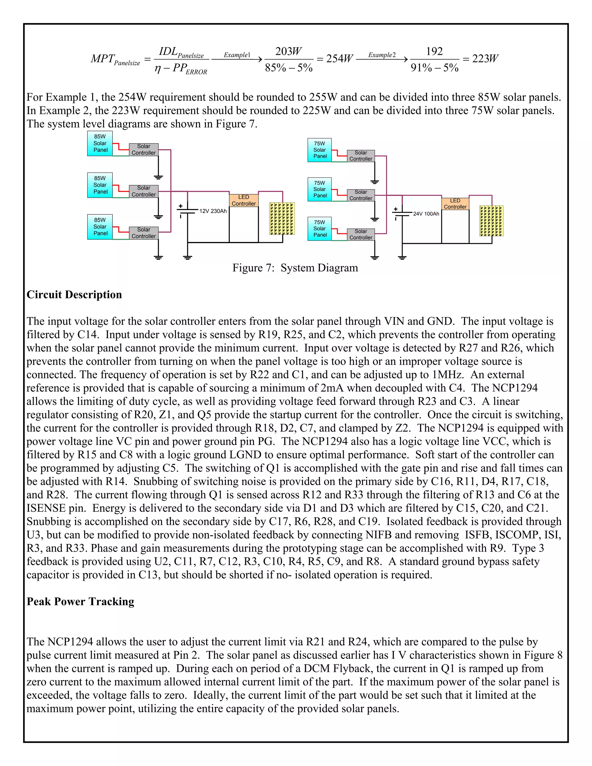
For Example 1, the 254W requirement should be rounded to 255W and can be divided into three 85W solar panels.
In Example 2, the 223W requirement should be rounded to 225W and can be divided into three 75W solar panels.
The system level diagrams are shown in Figure 7.
85W
Solar
Panel
85W
Solar
Panel
85W
Solar
Panel
Solar
Controller
Solar
Controller
Solar
Controller
12V 230Ah
LED
Controller
`
75W
Solar
Panel
75W
Solar
Panel
75W
Solar
Panel
Solar
Controller
Solar
Controller
Solar
Controller
24V 100Ah
LED
Controller
`
Figure 7: System Diagram
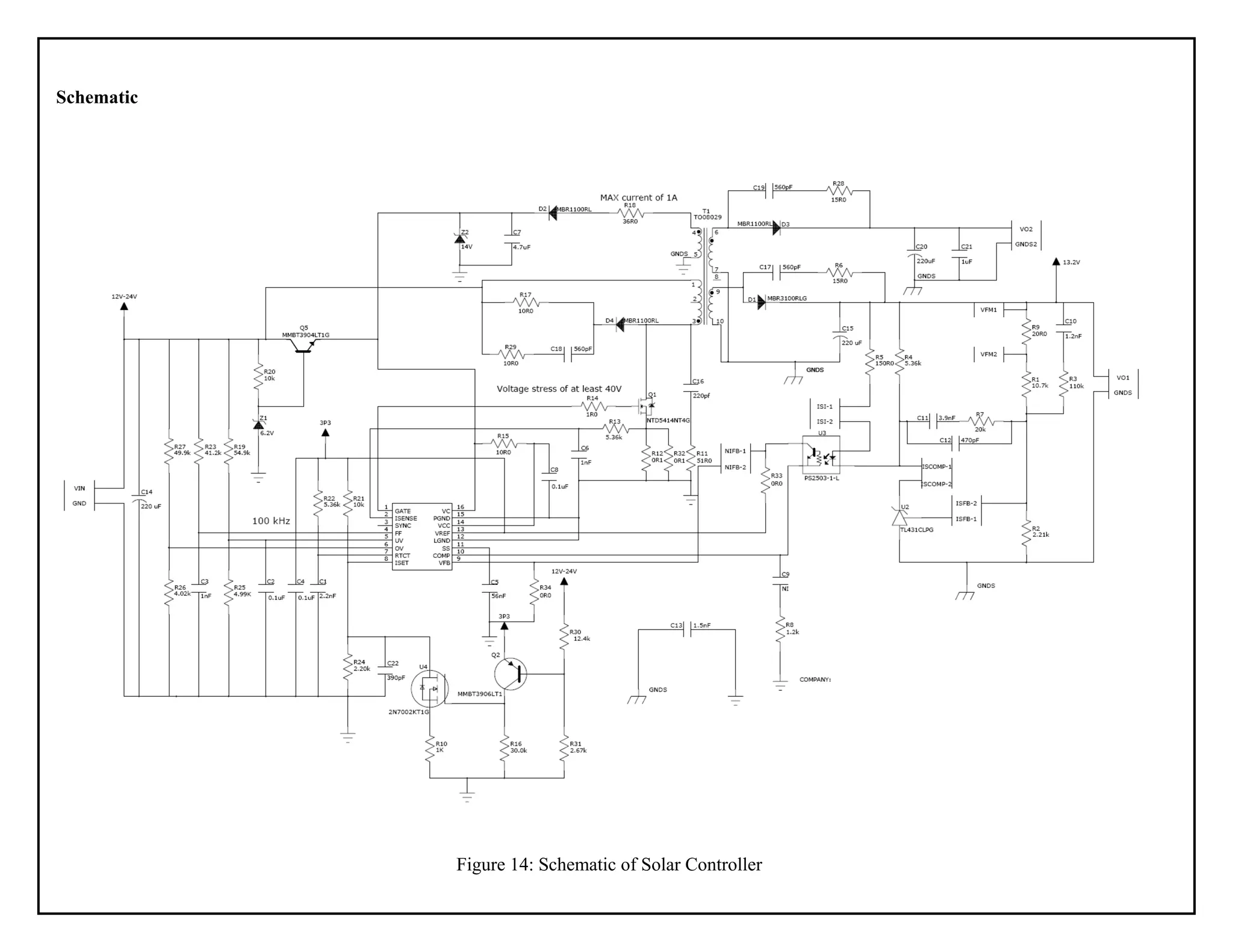
Circuit Description
The input voltage for the solar controller enters from the solar panel through VIN and GND. The input voltage is
filtered by C14. Input under voltage is sensed by R19, R25, and C2, which prevents the controller from operating
when the solar panel cannot provide the minimum current. Input over voltage is detected by R27 and R26, which
prevents the controller from turning on when the panel voltage is too high or an improper voltage source is
connected. The frequency of operation is set by R22 and C1, and can be adjusted up to 1MHz. An external
reference is provided that is capable of sourcing a minimum of 2mA when decoupled with C4. The NCP1294
allows the limiting of duty cycle, as well as providing voltage feed forward through R23 and C3. A linear
regulator consisting of R20, Z1, and Q5 provide the startup current for the controller. Once the circuit is switching,
the current for the controller is provided through R18, D2, C7, and clamped by Z2. The NCP1294 is equipped with
power voltage line VC pin and power ground pin PG. The NCP1294 also has a logic voltage line VCC, which is
filtered by R15 and C8 with a logic ground LGND to ensure optimal performance. Soft start of the controller can
be programmed by adjusting C5. The switching of Q1 is accomplished with the gate pin and rise and fall times can
be adjusted with R14. Snubbing of switching noise is provided on the primary side by C16, R11, D4, R17, C18,
and R28. The current flowing through Q1 is sensed across R12 and R33 through the filtering of R13 and C6 at the
ISENSE pin. Energy is delivered to the secondary side via D1 and D3 which are filtered by C15, C20, and C21.
Snubbing is accomplished on the secondary side by C17, R6, R28, and C19. Isolated feedback is provided through
U3, but can be modified to provide non-isolated feedback by connecting NIFB and removing ISFB, ISCOMP, ISI,
R3, and R33. Phase and gain measurements during the prototyping stage can be accomplished with R9. Type 3
feedback is provided using U2, C11, R7, C12, R3, C10, R4, R5, C9, and R8. A standard ground bypass safety
capacitor is provided in C13, but should be shorted if no- isolated operation is required.
Peak Power Tracking
The NCP1294 allows the user to adjust the current limit via R21 and R24, which are compared to the pulse by
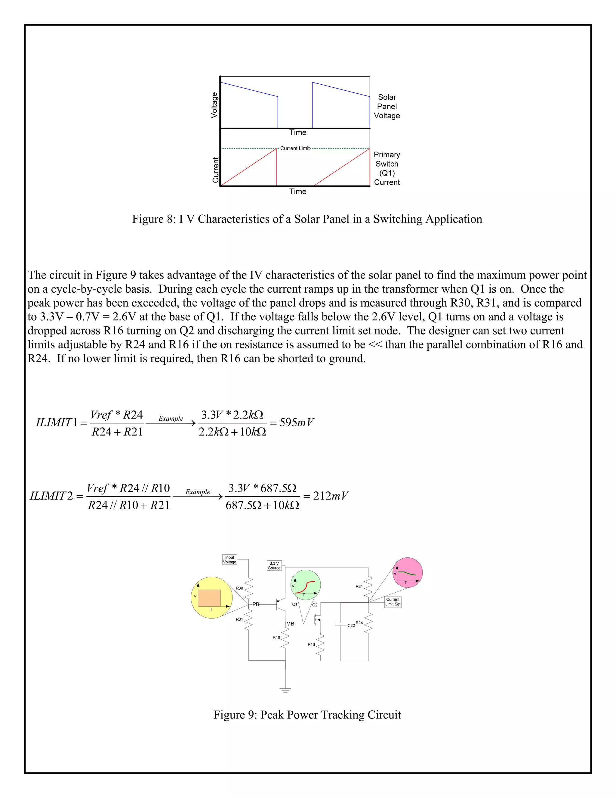
pulse current limit measured at Pin 2. The solar panel as discussed earlier has I V characteristics shown in Figure 8
when the current is ramped up. During each on period of a DCM Flyback, the current in Q1 is ramped up from
zero current to the maximum allowed internal current limit of the part. If the maximum power of the solar panel is
exceeded, the voltage falls to zero. Ideally, the current limit of the part would be set such that it limited at the
maximum power point, utilizing the entire capacity of the provided solar panels.
Figure 8: I V Characteristics of a Solar Panel in a Switching Application
The circuit in Figure 9 takes advantage of the IV characteristics of the solar panel to find the maximum power point
on a cycle-by-cycle basis. During each cycle the current ramps up in the transformer when Q1 is on. Once the
peak power has been exceeded, the voltage of the panel drops and is measured through R30, R31, and is compared
to 3.3V – 0.7V = 2.6V at the base of Q1. If the voltage falls below the 2.6V level, Q1 turns on and a voltage is
dropped across R16 turning on Q2 and discharging the current limit set node. The designer can set two current
limits adjustable by R24 and R16 if the on resistance is assumed to be << than the parallel combination of R16 and
R24. If no lower limit is required, then R16 can be shorted to ground.
mV
kk
kV
RR
RVref
ILIMIT Example
595
102.2
2.2*3.3
2124
24*
1 =
Ω+Ω
Ω
⎯⎯⎯ →⎯
+
=
mV
k
V
RRR
RRVref
ILIMIT Example
212
105.687
5.687*3.3
2110//24
10//24*
2 =
Ω+Ω
Ω
⎯⎯⎯ →⎯
+
=
Figure 9: Peak Power Tracking Circuit
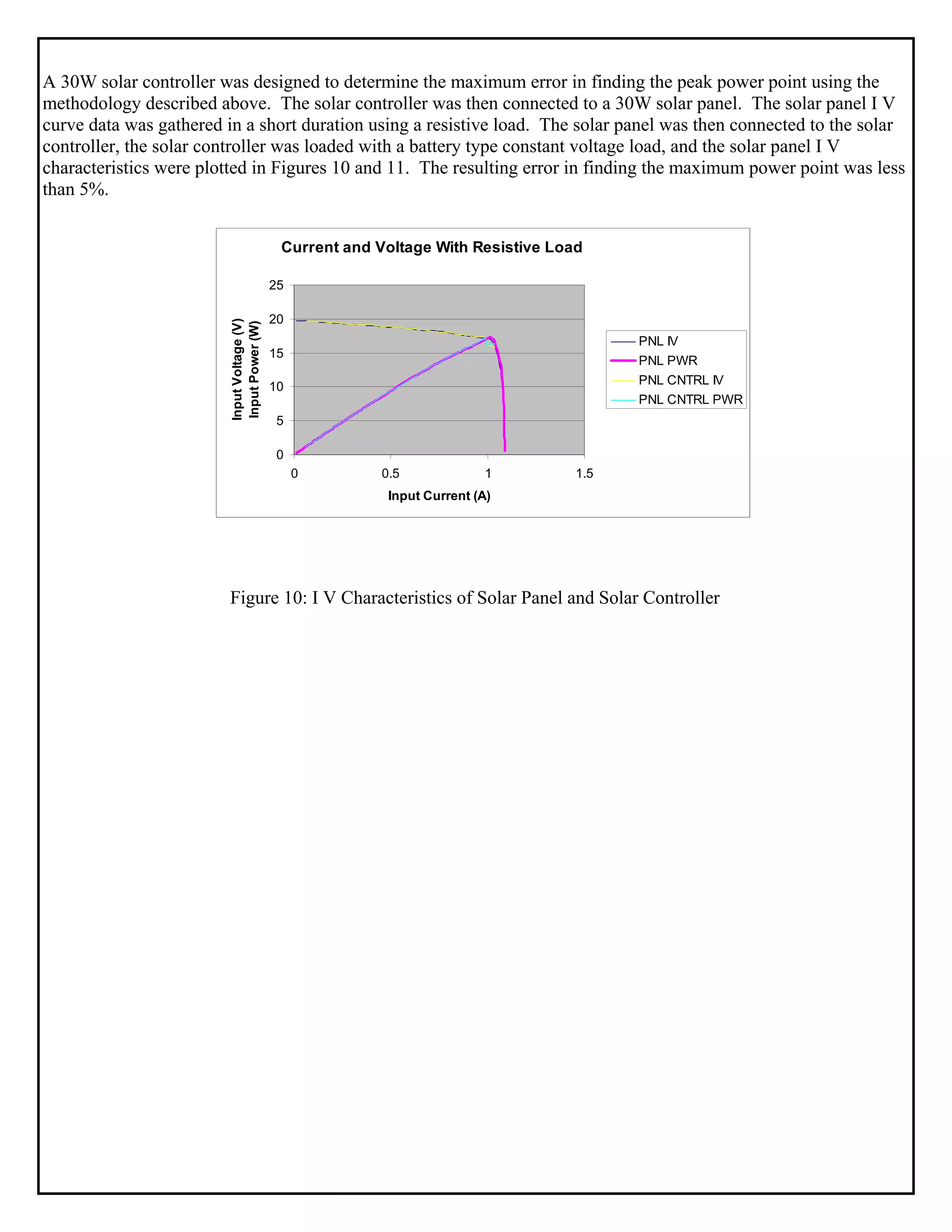
A 30W solar controller was designed to determine the maximum error in finding the peak power point using the
methodology described above. The solar controller was then connected to a 30W solar panel. The solar panel I V
curve data was gathered in a short duration using a resistive load. The solar panel was then connected to the solar
controller, the solar controller was loaded with a battery type constant voltage load, and the solar panel I V
characteristics were plotted in Figures 10 and 11. The resulting error in finding the maximum power point was less
than 5%.
Figure 10: I V Characteristics of Solar Panel and Solar Controller
Current and Voltage With Resistive Load and CS51221
0
5
10
15
20
25
0 0.5 1 1.5
Input Current (A)
InputVoltage(V)
InputPower(W)
PNL IV
PNL PWR
PNL CNTRL IV
PNL CNTRL PWR
Figure 11: I V Characteristics of Solar Panel and Solar Controller Error
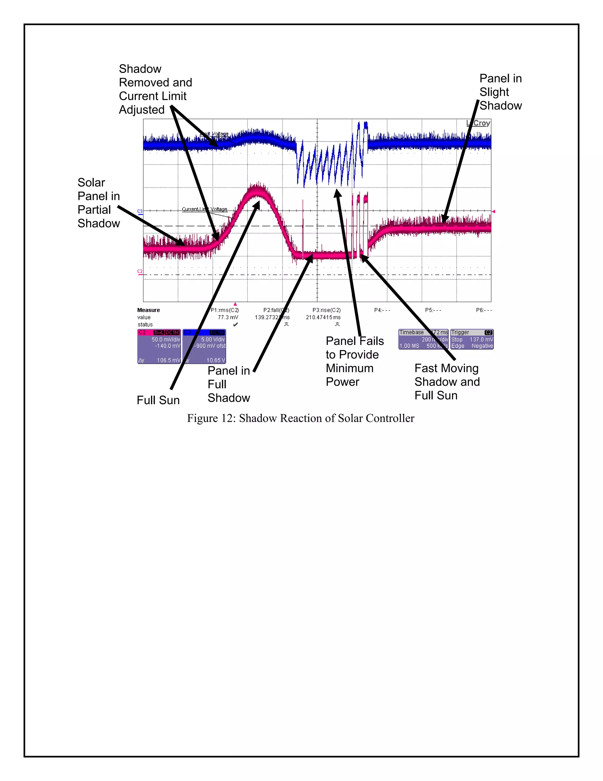
The control scheme should react and find the maximum power point in both the static and dynamic
cases. The street light may have been installed when trees were small and over time they may shade the
solar panel or have moving shadows that pass over the solar panel on windy day. Figure 12 shows the
case where a tree is casting a shadow on the solar panel, a gust of wind moves the leaves to expose the
solar panel to full sun, covers it completely, then provides the panel with more sun than the original
level, all taking place in less than 6 seconds.
Current and Voltage With Resistive Load and CS51221
14
14.5
15
15.5
16
16.5
17
17.5
0.8 0.9 1 1.1
Input Current (A)
InputPower(W)
PNL PWR
PNL CNTRL PWR
5% Error
Figure 12: Shadow Reaction of Solar Controller
Solar
Panel in
Partial
Shadow
Shadow
Removed and
Current Limit
Adjusted
Full Sun
Panel in
Full
Shadow
Panel Fails
to Provide
Minimum
Power
Panel in
Slight
Shadow
Fast Moving
Shadow and
Full Sun
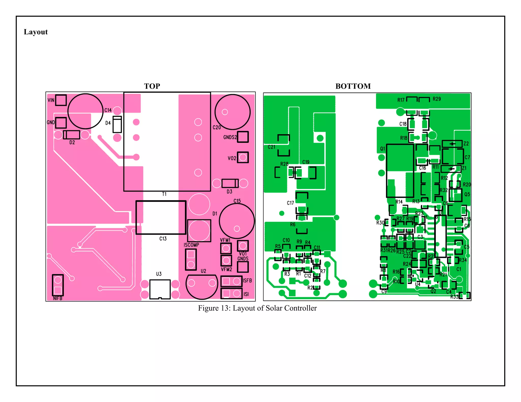
Layout
TOP BOTTOM
Figure 13: Layout of Solar Controller
Schematic
Figure 14: Schematic of Solar Controller
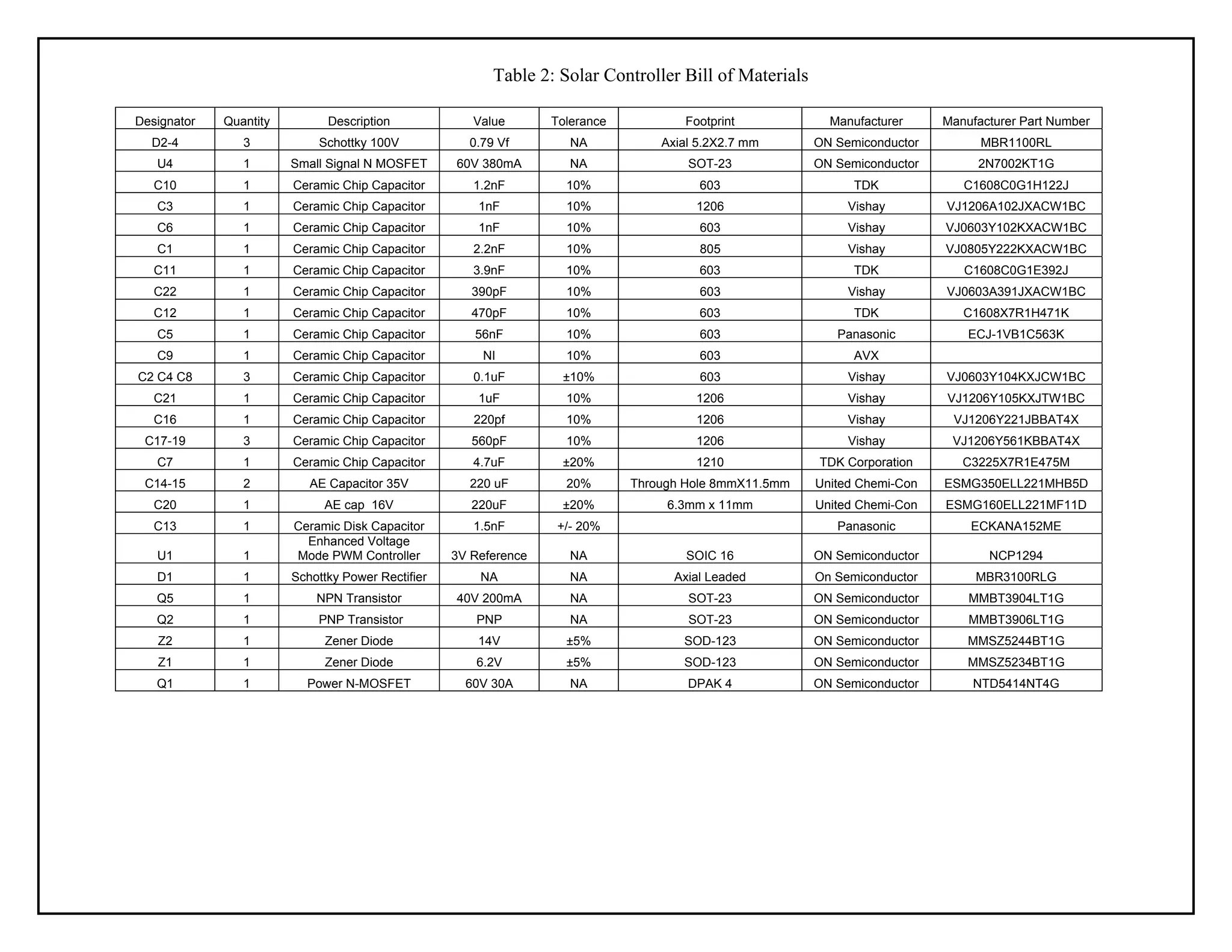
Table 2: Solar Controller Bill of Materials
Designator Quantity Description Value Tolerance Footprint Manufacturer Manufacturer Part Number
D2-4 3 Schottky 100V 0.79 Vf NA Axial 5.2X2.7 mm ON Semiconductor MBR1100RL
U4 1 Small Signal N MOSFET 60V 380mA NA SOT-23 ON Semiconductor 2N7002KT1G
C10 1 Ceramic Chip Capacitor 1.2nF 10% 603 TDK C1608C0G1H122J
C3 1 Ceramic Chip Capacitor 1nF 10% 1206 Vishay VJ1206A102JXACW1BC
C6 1 Ceramic Chip Capacitor 1nF 10% 603 Vishay VJ0603Y102KXACW1BC
C1 1 Ceramic Chip Capacitor 2.2nF 10% 805 Vishay VJ0805Y222KXACW1BC
C11 1 Ceramic Chip Capacitor 3.9nF 10% 603 TDK C1608C0G1E392J
C22 1 Ceramic Chip Capacitor 390pF 10% 603 Vishay VJ0603A391JXACW1BC
C12 1 Ceramic Chip Capacitor 470pF 10% 603 TDK C1608X7R1H471K
C5 1 Ceramic Chip Capacitor 56nF 10% 603 Panasonic ECJ-1VB1C563K
C9 1 Ceramic Chip Capacitor NI 10% 603 AVX
C2 C4 C8 3 Ceramic Chip Capacitor 0.1uF ±10% 603 Vishay VJ0603Y104KXJCW1BC
C21 1 Ceramic Chip Capacitor 1uF 10% 1206 Vishay VJ1206Y105KXJTW1BC
C16 1 Ceramic Chip Capacitor 220pf 10% 1206 Vishay VJ1206Y221JBBAT4X
C17-19 3 Ceramic Chip Capacitor 560pF 10% 1206 Vishay VJ1206Y561KBBAT4X
C7 1 Ceramic Chip Capacitor 4.7uF ±20% 1210 TDK Corporation C3225X7R1E475M
C14-15 2 AE Capacitor 35V 220 uF 20% Through Hole 8mmX11.5mm United Chemi-Con ESMG350ELL221MHB5D
C20 1 AE cap 16V 220uF ±20% 6.3mm x 11mm United Chemi-Con ESMG160ELL221MF11D
C13 1 Ceramic Disk Capacitor 1.5nF +/- 20% Panasonic ECKANA152ME
U1 1
Enhanced Voltage
Mode PWM Controller 3V Reference NA SOIC 16 ON Semiconductor NCP1294
D1 1 Schottky Power Rectifier NA NA Axial Leaded On Semiconductor MBR3100RLG
Q5 1 NPN Transistor 40V 200mA NA SOT-23 ON Semiconductor MMBT3904LT1G
Q2 1 PNP Transistor PNP NA SOT-23 ON Semiconductor MMBT3906LT1G
Z2 1 Zener Diode 14V ±5% SOD-123 ON Semiconductor MMSZ5244BT1G
Z1 1 Zener Diode 6.2V ±5% SOD-123 ON Semiconductor MMSZ5234BT1G
Q1 1 Power N-MOSFET 60V 30A NA DPAK 4 ON Semiconductor NTD5414NT4G
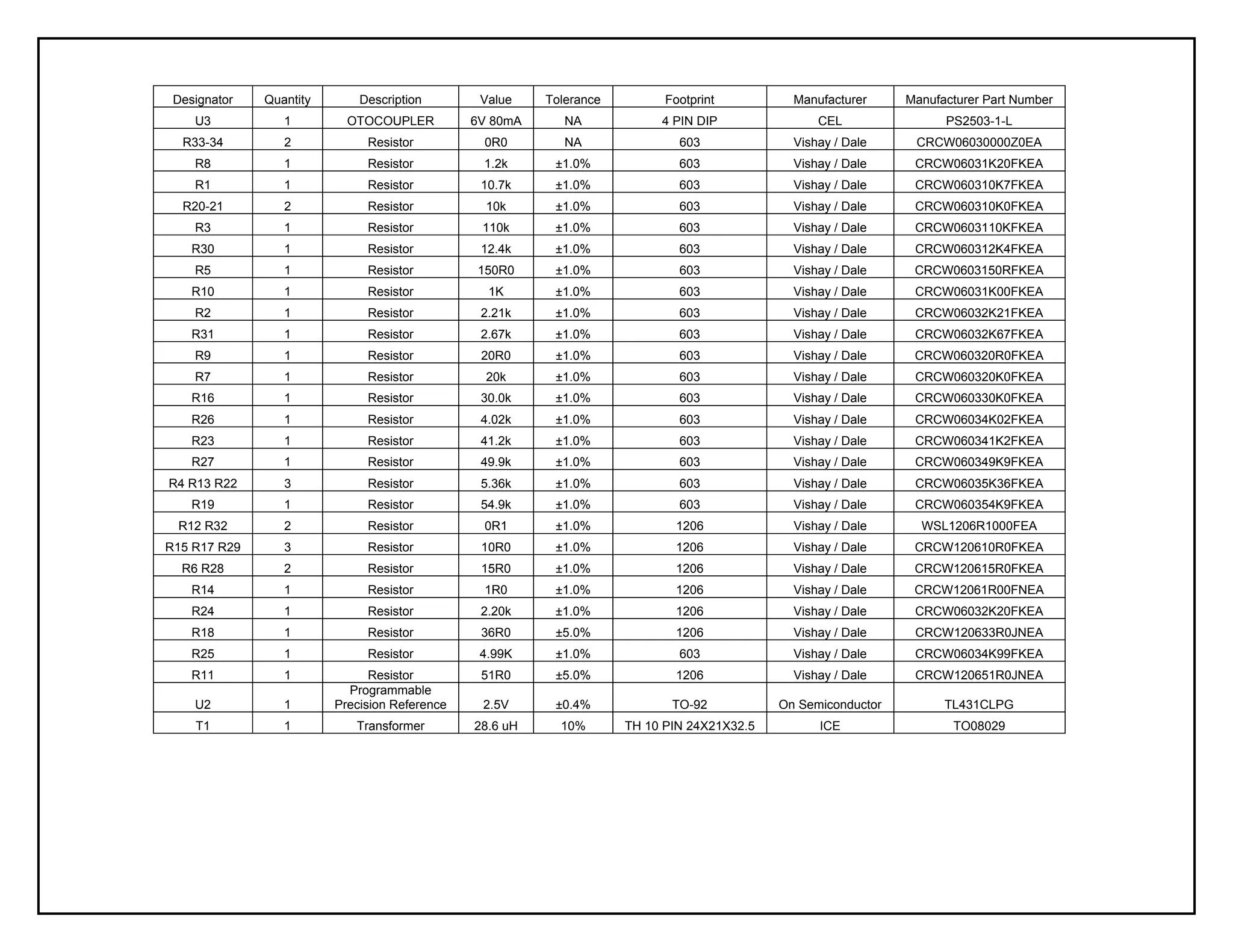
Designator Quantity Description Value Tolerance Footprint Manufacturer Manufacturer Part Number
U3 1 OTOCOUPLER 6V 80mA NA 4 PIN DIP CEL PS2503-1-L
R33-34 2 Resistor 0R0 NA 603 Vishay / Dale CRCW06030000Z0EA
R8 1 Resistor 1.2k ±1.0% 603 Vishay / Dale CRCW06031K20FKEA
R1 1 Resistor 10.7k ±1.0% 603 Vishay / Dale CRCW060310K7FKEA
R20-21 2 Resistor 10k ±1.0% 603 Vishay / Dale CRCW060310K0FKEA
R3 1 Resistor 110k ±1.0% 603 Vishay / Dale CRCW0603110KFKEA
R30 1 Resistor 12.4k ±1.0% 603 Vishay / Dale CRCW060312K4FKEA
R5 1 Resistor 150R0 ±1.0% 603 Vishay / Dale CRCW0603150RFKEA
R10 1 Resistor 1K ±1.0% 603 Vishay / Dale CRCW06031K00FKEA
R2 1 Resistor 2.21k ±1.0% 603 Vishay / Dale CRCW06032K21FKEA
R31 1 Resistor 2.67k ±1.0% 603 Vishay / Dale CRCW06032K67FKEA
R9 1 Resistor 20R0 ±1.0% 603 Vishay / Dale CRCW060320R0FKEA
R7 1 Resistor 20k ±1.0% 603 Vishay / Dale CRCW060320K0FKEA
R16 1 Resistor 30.0k ±1.0% 603 Vishay / Dale CRCW060330K0FKEA
R26 1 Resistor 4.02k ±1.0% 603 Vishay / Dale CRCW06034K02FKEA
R23 1 Resistor 41.2k ±1.0% 603 Vishay / Dale CRCW060341K2FKEA
R27 1 Resistor 49.9k ±1.0% 603 Vishay / Dale CRCW060349K9FKEA
R4 R13 R22 3 Resistor 5.36k ±1.0% 603 Vishay / Dale CRCW06035K36FKEA
R19 1 Resistor 54.9k ±1.0% 603 Vishay / Dale CRCW060354K9FKEA
R12 R32 2 Resistor 0R1 ±1.0% 1206 Vishay / Dale WSL1206R1000FEA
R15 R17 R29 3 Resistor 10R0 ±1.0% 1206 Vishay / Dale CRCW120610R0FKEA
R6 R28 2 Resistor 15R0 ±1.0% 1206 Vishay / Dale CRCW120615R0FKEA
R14 1 Resistor 1R0 ±1.0% 1206 Vishay / Dale CRCW12061R00FNEA
R24 1 Resistor 2.20k ±1.0% 1206 Vishay / Dale CRCW06032K20FKEA
R18 1 Resistor 36R0 ±5.0% 1206 Vishay / Dale CRCW120633R0JNEA
R25 1 Resistor 4.99K ±1.0% 603 Vishay / Dale CRCW06034K99FKEA
R11 1 Resistor 51R0 ±5.0% 1206 Vishay / Dale CRCW120651R0JNEA
U2 1
Programmable
Precision Reference 2.5V ±0.4% TO-92 On Semiconductor TL431CLPG
T1 1 Transformer 28.6 uH 10% TH 10 PIN 24X21X32.5 ICE TO08029
May 2009, Rev.1 www.onsemi.com 13
[1] NREL National Renewable Energy Laboratory webpage. 2008
<http://www.nrel.gov/gis/solar.html>
1
© 2009 ON Semiconductor.
Disclaimer: ON Semiconductor is providing this design note “AS IS” and does not assume any liability arising from its use;
nor does ON Semiconductor convey any license to its or any third party’s intellectual property rights. This document is
provided only to assist customers in evaluation of the referenced circuit implementation and the recipient assumes all liability
and risk associated with its use, including, but not limited to, compliance with all regulatory standards. ON Semiconductor
may change any of its products at any time, without notice.
Design note created by Tim Kaske and Bryan McCoy, e-mail: Tim.Kaske@onsemi.com ;
Bryan.McCoy@onsemi.com

Solar power mppt controller

  • 1.
    Design Note –DN06054/D Reference Design for Solar Power MPPT Controller Device Application Input Voltage Output Voltage Output Current Topology NCP1294 Solar Street Lighting 12-24 V A 13.2V A 2.0A Flyback Table 1: NCP1294 Output Statistics Characteristic Min Typ Max Unit Output Voltage 9 12 13.5 V Output Current 0 2.0 A Oscillator Frequency 100 kHz 1. < 2mA Current Consumption from Battery 2. Maximum Power Tracking < 5% Error 3. Can Charge 4 Batteries in Series or Parallel 4. Can be Configured for use with 10W to 30W Solar Panels 5. Can be used in Parallel with Other Systems Figure 1: Solar Controller Evaluation Board
  • 2.
    System Description The systemunder consideration is an off grid solar streetlamp. The solar streetlamp consists of high power LEDS, a lead acid battery, a solar controller, and a solar panel as shown in Figure 2. Solar Controller 12V+ - Solar Panel Solar Controller Lead Acid Battery LED Street Light Figure 2: Basic off Grid Solar Streetlamp System Solar Panel Characteristics Solar panels collect energy from the sun and convert it to electrical energy. Unfortunately, the sun is not consistent throughout the day due to cloud cover and the angle of the sun relative to the position of the solar panel. Further, the intensity of the sun varies with the season, geographic location, and reflections from adjacent surfaces. Figure 3 shows the monthly average daily total solar resource information on grid cells of approximately 40 km by 40 km in size [1]. Figure 3: Monthly Average Daily Total Solar Resource in December (Right) and July (Left) [1] Since the sun is not consistent, the solar panel rated for 30W peak power may only supply 24W in midday sun and 6 W in the evening sun. Figure 4 displays the voltage, current, and power characteristics of a solar panel at various times during the day with a resistive load. The voltage from solar panels can be configured by the manufacturer to supply almost any voltage and current depending on the solar cell configuration, but generally range from 20V to 48V.
  • 3.
    Solar Panel INMiday Sun 0 2 4 6 8 10 12 14 16 18 20 22 24 0 0.2 0.4 0.6 0.8 1 1.2 1.4 1.6 1.8 2 Current(I) Voltage(V)/ Power(W) Voltage Power Solar Panel Power in Afternoon Sun 0 2 4 6 8 10 12 14 16 18 20 0 0.2 0.4 0.6 0.8 1 1.2 1.4 Current(I) Voltage(V)/ Power(W) Voltage Power Solar Panel in Evening Sun 0 2 4 6 8 10 12 14 16 18 20 0 0.2 0.4 0.6 Current(I) Voltage(V)/ Power(W) Voltage Power Figure 4: Solar Panel Available Power at Midday (Left) Afternoon (Middle) and Evening (Right) Controller Considerations When designing the solar street lighting system, the worst-case scenarios must be considered if the light provided is for safety rather than convenience. Solar energy is measured in hours of the day at which the maximum rated performance from a solar panel can be obtained (peak_power_time). On average, Arizona has six peak hours of sun daily. Solar panels are rated for the peak power they produce, thus the required energy from solar panels can be calculated since the required load energy is known. Excess solar capacity needs to be considered for charge recovery from a cloudy day giving the designer a fixed number of days from which to recover from a series of cloudy days (Recharge-Time). W h Wh W h Wh TimePowerPeak LoadEnergy IDL ExampleExample Panelsize 112 6 672 119 6 712 __ 21 =⎯⎯⎯ →⎯=⎯⎯⎯ →⎯= W kW W kW timeech acityBatteryCap RECHARGE ExampleExample Panelsize 80 30 4.2 84 30 .2 _argRe 21 =⎯⎯⎯ →⎯=⎯⎯⎯ →⎯ WWW WWWIDLRECHARGETotal Example Example PanelsizePanelsizePanelsize 19280112 20384119 2 1 =+⎯⎯⎯ →⎯ =+⎯⎯⎯ →⎯+= The designer need only extract the peak power, deliver it to the battery, and then the system will be complete. Unfortunately, the solar panel characteristics make it difficult to find the peak power point as it moves with many variables. If the solar panel is simply connected to the battery and removed once it is charged, 20% - 30% of the peak power is lost depending on the state of charge of the battery. Commonly solar panels are the most expensive part of the system averaging $4/W/USD. Solar panels are typically manufactured in 5W increments, thus each increment in power costs $20/USD. The price of a linear charge controller may look attractive from the piece part standpoint, but may end with a less cost effective system. The panel size required for a linear charging system is calculated below. W W W W PPLIN Total LINEAR ExampleExample LossEFF Panelsize Panelsize 274 25.095.0 192 290 25.095.0 203 21 = − ⎯⎯⎯ →⎯= − ⎯⎯⎯ →⎯ − = The discrepancy between the peak power and the linear regulator power is 87W and 82W. If an algorithm for peak power tracking is implemented, there will be an error from the true peak power point and the algorithm operating point. The peak power error (PPerror) operation point results in unused energy from the solar panel, so the smaller the percentage of error, the greater the power extracted. The solar controller efficiency operates at 88% for the 12V system and 91% for the 24V system. The required solar panel size with peak power tracking is calculated below.
  • 4.
    WW W PP IDL MPT ExampleExample ERROR Panelsize Panelsize 223 %5%91 192 254 %5%85 20321 = − ⎯⎯⎯ →⎯= − ⎯⎯⎯ →⎯ − = η For Example 1, the 254W requirement should be rounded to 255W and can be divided into three 85W solar panels. In Example 2, the 223W requirement should be rounded to 225W and can be divided into three 75W solar panels. The system level diagrams are shown in Figure 7. 85W Solar Panel 85W Solar Panel 85W Solar Panel Solar Controller Solar Controller Solar Controller 12V 230Ah LED Controller ` 75W Solar Panel 75W Solar Panel 75W Solar Panel Solar Controller Solar Controller Solar Controller 24V 100Ah LED Controller ` Figure 7: System Diagram Circuit Description The input voltage for the solar controller enters from the solar panel through VIN and GND. The input voltage is filtered by C14. Input under voltage is sensed by R19, R25, and C2, which prevents the controller from operating when the solar panel cannot provide the minimum current. Input over voltage is detected by R27 and R26, which prevents the controller from turning on when the panel voltage is too high or an improper voltage source is connected. The frequency of operation is set by R22 and C1, and can be adjusted up to 1MHz. An external reference is provided that is capable of sourcing a minimum of 2mA when decoupled with C4. The NCP1294 allows the limiting of duty cycle, as well as providing voltage feed forward through R23 and C3. A linear regulator consisting of R20, Z1, and Q5 provide the startup current for the controller. Once the circuit is switching, the current for the controller is provided through R18, D2, C7, and clamped by Z2. The NCP1294 is equipped with power voltage line VC pin and power ground pin PG. The NCP1294 also has a logic voltage line VCC, which is filtered by R15 and C8 with a logic ground LGND to ensure optimal performance. Soft start of the controller can be programmed by adjusting C5. The switching of Q1 is accomplished with the gate pin and rise and fall times can be adjusted with R14. Snubbing of switching noise is provided on the primary side by C16, R11, D4, R17, C18, and R28. The current flowing through Q1 is sensed across R12 and R33 through the filtering of R13 and C6 at the ISENSE pin. Energy is delivered to the secondary side via D1 and D3 which are filtered by C15, C20, and C21. Snubbing is accomplished on the secondary side by C17, R6, R28, and C19. Isolated feedback is provided through U3, but can be modified to provide non-isolated feedback by connecting NIFB and removing ISFB, ISCOMP, ISI, R3, and R33. Phase and gain measurements during the prototyping stage can be accomplished with R9. Type 3 feedback is provided using U2, C11, R7, C12, R3, C10, R4, R5, C9, and R8. A standard ground bypass safety capacitor is provided in C13, but should be shorted if no- isolated operation is required. Peak Power Tracking The NCP1294 allows the user to adjust the current limit via R21 and R24, which are compared to the pulse by pulse current limit measured at Pin 2. The solar panel as discussed earlier has I V characteristics shown in Figure 8 when the current is ramped up. During each on period of a DCM Flyback, the current in Q1 is ramped up from zero current to the maximum allowed internal current limit of the part. If the maximum power of the solar panel is exceeded, the voltage falls to zero. Ideally, the current limit of the part would be set such that it limited at the maximum power point, utilizing the entire capacity of the provided solar panels.
  • 5.
    Figure 8: IV Characteristics of a Solar Panel in a Switching Application The circuit in Figure 9 takes advantage of the IV characteristics of the solar panel to find the maximum power point on a cycle-by-cycle basis. During each cycle the current ramps up in the transformer when Q1 is on. Once the peak power has been exceeded, the voltage of the panel drops and is measured through R30, R31, and is compared to 3.3V – 0.7V = 2.6V at the base of Q1. If the voltage falls below the 2.6V level, Q1 turns on and a voltage is dropped across R16 turning on Q2 and discharging the current limit set node. The designer can set two current limits adjustable by R24 and R16 if the on resistance is assumed to be << than the parallel combination of R16 and R24. If no lower limit is required, then R16 can be shorted to ground. mV kk kV RR RVref ILIMIT Example 595 102.2 2.2*3.3 2124 24* 1 = Ω+Ω Ω ⎯⎯⎯ →⎯ + = mV k V RRR RRVref ILIMIT Example 212 105.687 5.687*3.3 2110//24 10//24* 2 = Ω+Ω Ω ⎯⎯⎯ →⎯ + = Figure 9: Peak Power Tracking Circuit
  • 6.
    A 30W solarcontroller was designed to determine the maximum error in finding the peak power point using the methodology described above. The solar controller was then connected to a 30W solar panel. The solar panel I V curve data was gathered in a short duration using a resistive load. The solar panel was then connected to the solar controller, the solar controller was loaded with a battery type constant voltage load, and the solar panel I V characteristics were plotted in Figures 10 and 11. The resulting error in finding the maximum power point was less than 5%. Figure 10: I V Characteristics of Solar Panel and Solar Controller Current and Voltage With Resistive Load and CS51221 0 5 10 15 20 25 0 0.5 1 1.5 Input Current (A) InputVoltage(V) InputPower(W) PNL IV PNL PWR PNL CNTRL IV PNL CNTRL PWR
  • 7.
    Figure 11: IV Characteristics of Solar Panel and Solar Controller Error The control scheme should react and find the maximum power point in both the static and dynamic cases. The street light may have been installed when trees were small and over time they may shade the solar panel or have moving shadows that pass over the solar panel on windy day. Figure 12 shows the case where a tree is casting a shadow on the solar panel, a gust of wind moves the leaves to expose the solar panel to full sun, covers it completely, then provides the panel with more sun than the original level, all taking place in less than 6 seconds. Current and Voltage With Resistive Load and CS51221 14 14.5 15 15.5 16 16.5 17 17.5 0.8 0.9 1 1.1 Input Current (A) InputPower(W) PNL PWR PNL CNTRL PWR 5% Error
  • 8.
    Figure 12: ShadowReaction of Solar Controller Solar Panel in Partial Shadow Shadow Removed and Current Limit Adjusted Full Sun Panel in Full Shadow Panel Fails to Provide Minimum Power Panel in Slight Shadow Fast Moving Shadow and Full Sun
  • 9.
    Layout TOP BOTTOM Figure 13:Layout of Solar Controller
  • 10.
    Schematic Figure 14: Schematicof Solar Controller
  • 11.
    Table 2: SolarController Bill of Materials Designator Quantity Description Value Tolerance Footprint Manufacturer Manufacturer Part Number D2-4 3 Schottky 100V 0.79 Vf NA Axial 5.2X2.7 mm ON Semiconductor MBR1100RL U4 1 Small Signal N MOSFET 60V 380mA NA SOT-23 ON Semiconductor 2N7002KT1G C10 1 Ceramic Chip Capacitor 1.2nF 10% 603 TDK C1608C0G1H122J C3 1 Ceramic Chip Capacitor 1nF 10% 1206 Vishay VJ1206A102JXACW1BC C6 1 Ceramic Chip Capacitor 1nF 10% 603 Vishay VJ0603Y102KXACW1BC C1 1 Ceramic Chip Capacitor 2.2nF 10% 805 Vishay VJ0805Y222KXACW1BC C11 1 Ceramic Chip Capacitor 3.9nF 10% 603 TDK C1608C0G1E392J C22 1 Ceramic Chip Capacitor 390pF 10% 603 Vishay VJ0603A391JXACW1BC C12 1 Ceramic Chip Capacitor 470pF 10% 603 TDK C1608X7R1H471K C5 1 Ceramic Chip Capacitor 56nF 10% 603 Panasonic ECJ-1VB1C563K C9 1 Ceramic Chip Capacitor NI 10% 603 AVX C2 C4 C8 3 Ceramic Chip Capacitor 0.1uF ±10% 603 Vishay VJ0603Y104KXJCW1BC C21 1 Ceramic Chip Capacitor 1uF 10% 1206 Vishay VJ1206Y105KXJTW1BC C16 1 Ceramic Chip Capacitor 220pf 10% 1206 Vishay VJ1206Y221JBBAT4X C17-19 3 Ceramic Chip Capacitor 560pF 10% 1206 Vishay VJ1206Y561KBBAT4X C7 1 Ceramic Chip Capacitor 4.7uF ±20% 1210 TDK Corporation C3225X7R1E475M C14-15 2 AE Capacitor 35V 220 uF 20% Through Hole 8mmX11.5mm United Chemi-Con ESMG350ELL221MHB5D C20 1 AE cap 16V 220uF ±20% 6.3mm x 11mm United Chemi-Con ESMG160ELL221MF11D C13 1 Ceramic Disk Capacitor 1.5nF +/- 20% Panasonic ECKANA152ME U1 1 Enhanced Voltage Mode PWM Controller 3V Reference NA SOIC 16 ON Semiconductor NCP1294 D1 1 Schottky Power Rectifier NA NA Axial Leaded On Semiconductor MBR3100RLG Q5 1 NPN Transistor 40V 200mA NA SOT-23 ON Semiconductor MMBT3904LT1G Q2 1 PNP Transistor PNP NA SOT-23 ON Semiconductor MMBT3906LT1G Z2 1 Zener Diode 14V ±5% SOD-123 ON Semiconductor MMSZ5244BT1G Z1 1 Zener Diode 6.2V ±5% SOD-123 ON Semiconductor MMSZ5234BT1G Q1 1 Power N-MOSFET 60V 30A NA DPAK 4 ON Semiconductor NTD5414NT4G
  • 12.
    Designator Quantity DescriptionValue Tolerance Footprint Manufacturer Manufacturer Part Number U3 1 OTOCOUPLER 6V 80mA NA 4 PIN DIP CEL PS2503-1-L R33-34 2 Resistor 0R0 NA 603 Vishay / Dale CRCW06030000Z0EA R8 1 Resistor 1.2k ±1.0% 603 Vishay / Dale CRCW06031K20FKEA R1 1 Resistor 10.7k ±1.0% 603 Vishay / Dale CRCW060310K7FKEA R20-21 2 Resistor 10k ±1.0% 603 Vishay / Dale CRCW060310K0FKEA R3 1 Resistor 110k ±1.0% 603 Vishay / Dale CRCW0603110KFKEA R30 1 Resistor 12.4k ±1.0% 603 Vishay / Dale CRCW060312K4FKEA R5 1 Resistor 150R0 ±1.0% 603 Vishay / Dale CRCW0603150RFKEA R10 1 Resistor 1K ±1.0% 603 Vishay / Dale CRCW06031K00FKEA R2 1 Resistor 2.21k ±1.0% 603 Vishay / Dale CRCW06032K21FKEA R31 1 Resistor 2.67k ±1.0% 603 Vishay / Dale CRCW06032K67FKEA R9 1 Resistor 20R0 ±1.0% 603 Vishay / Dale CRCW060320R0FKEA R7 1 Resistor 20k ±1.0% 603 Vishay / Dale CRCW060320K0FKEA R16 1 Resistor 30.0k ±1.0% 603 Vishay / Dale CRCW060330K0FKEA R26 1 Resistor 4.02k ±1.0% 603 Vishay / Dale CRCW06034K02FKEA R23 1 Resistor 41.2k ±1.0% 603 Vishay / Dale CRCW060341K2FKEA R27 1 Resistor 49.9k ±1.0% 603 Vishay / Dale CRCW060349K9FKEA R4 R13 R22 3 Resistor 5.36k ±1.0% 603 Vishay / Dale CRCW06035K36FKEA R19 1 Resistor 54.9k ±1.0% 603 Vishay / Dale CRCW060354K9FKEA R12 R32 2 Resistor 0R1 ±1.0% 1206 Vishay / Dale WSL1206R1000FEA R15 R17 R29 3 Resistor 10R0 ±1.0% 1206 Vishay / Dale CRCW120610R0FKEA R6 R28 2 Resistor 15R0 ±1.0% 1206 Vishay / Dale CRCW120615R0FKEA R14 1 Resistor 1R0 ±1.0% 1206 Vishay / Dale CRCW12061R00FNEA R24 1 Resistor 2.20k ±1.0% 1206 Vishay / Dale CRCW06032K20FKEA R18 1 Resistor 36R0 ±5.0% 1206 Vishay / Dale CRCW120633R0JNEA R25 1 Resistor 4.99K ±1.0% 603 Vishay / Dale CRCW06034K99FKEA R11 1 Resistor 51R0 ±5.0% 1206 Vishay / Dale CRCW120651R0JNEA U2 1 Programmable Precision Reference 2.5V ±0.4% TO-92 On Semiconductor TL431CLPG T1 1 Transformer 28.6 uH 10% TH 10 PIN 24X21X32.5 ICE TO08029
  • 13.
    May 2009, Rev.1www.onsemi.com 13 [1] NREL National Renewable Energy Laboratory webpage. 2008 <http://www.nrel.gov/gis/solar.html> 1 © 2009 ON Semiconductor. Disclaimer: ON Semiconductor is providing this design note “AS IS” and does not assume any liability arising from its use; nor does ON Semiconductor convey any license to its or any third party’s intellectual property rights. This document is provided only to assist customers in evaluation of the referenced circuit implementation and the recipient assumes all liability and risk associated with its use, including, but not limited to, compliance with all regulatory standards. ON Semiconductor may change any of its products at any time, without notice. Design note created by Tim Kaske and Bryan McCoy, e-mail: Tim.Kaske@onsemi.com ; Bryan.McCoy@onsemi.com