Advanced Computer Architecture
23MCAC105
by
Dr. S.K. Manju bargavi
Professor
Text & Reference Books
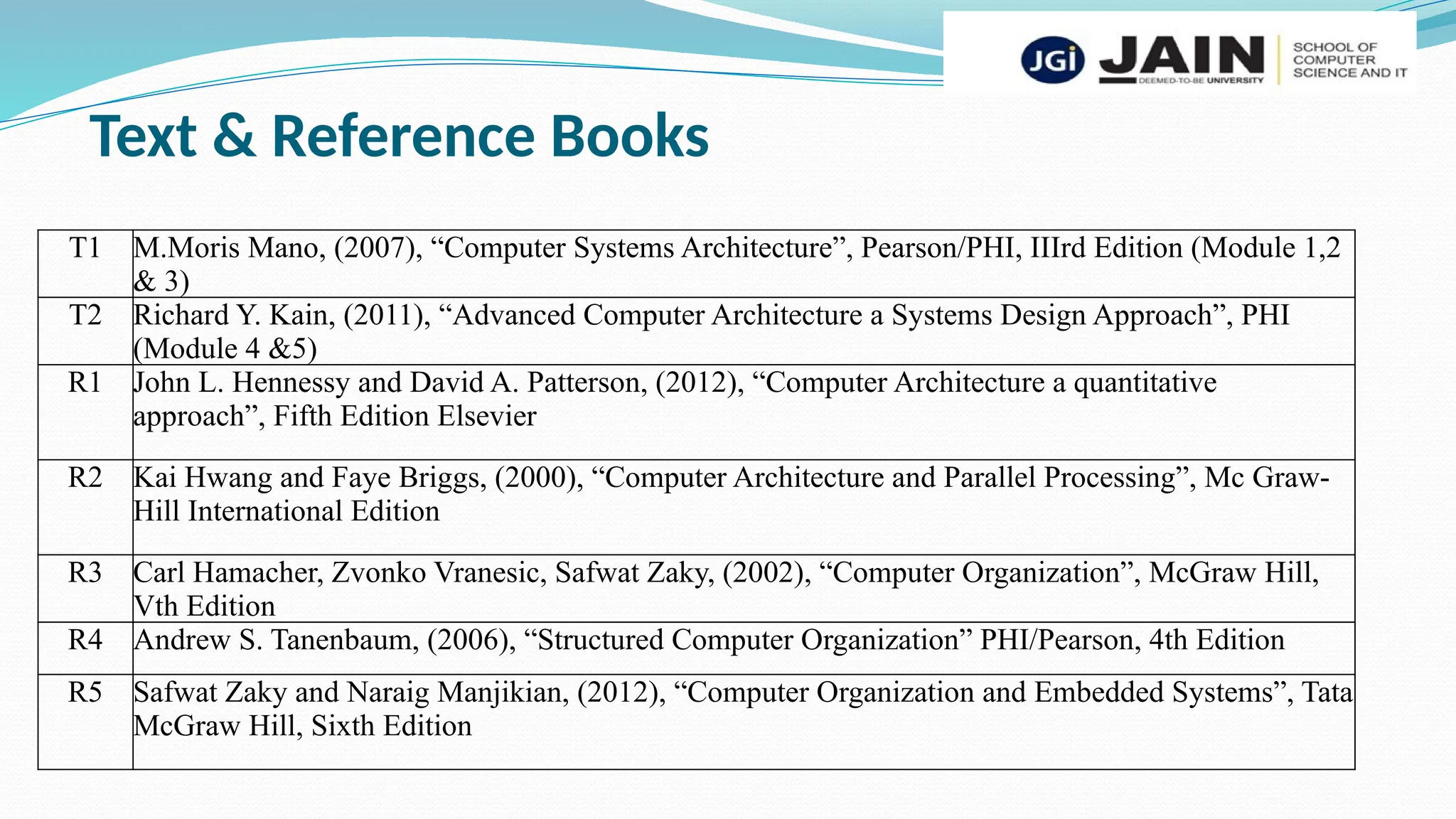
T1 M.Moris Mano, (2007), “Computer Systems Architecture”, Pearson/PHI, IIIrd Edition (Module 1,2
& 3)
T2 Richard Y. Kain, (2011), “Advanced Computer Architecture a Systems Design Approach”, PHI
(Module 4 &5)
R1 John L. Hennessy and David A. Patterson, (2012), “Computer Architecture a quantitative
approach”, Fifth Edition Elsevier
R2 Kai Hwang and Faye Briggs, (2000), “Computer Architecture and Parallel Processing”, Mc Graw-
Hill International Edition
R3 Carl Hamacher, Zvonko Vranesic, Safwat Zaky, (2002), “Computer Organization”, McGraw Hill,
Vth Edition
R4 Andrew S. Tanenbaum, (2006), “Structured Computer Organization” PHI/Pearson, 4th Edition
R5 Safwat Zaky and Naraig Manjikian, (2012), “Computer Organization and Embedded Systems”, Tata
McGraw Hill, Sixth Edition
Introduction
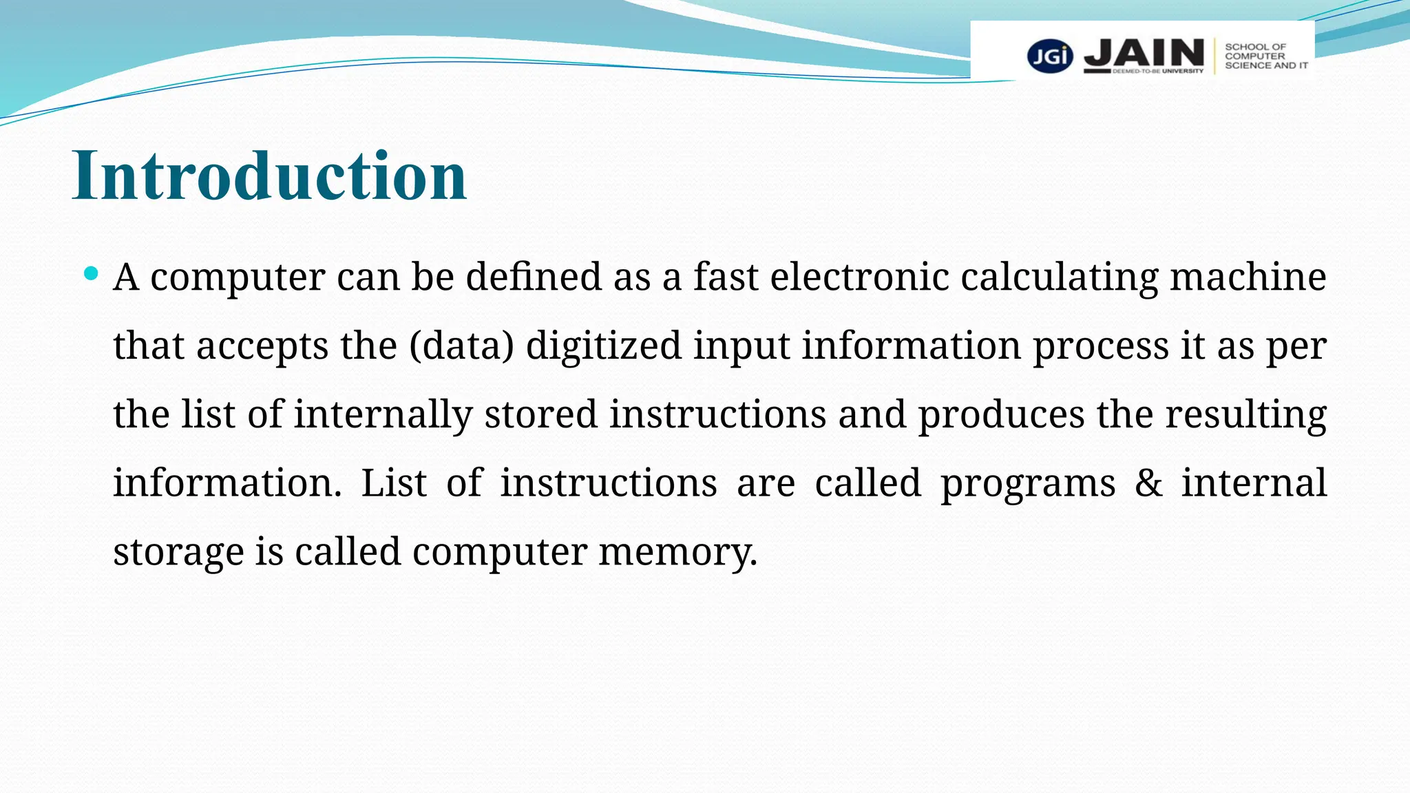
 A computer can be defined as a fast electronic calculating machine
that accepts the (data) digitized input information process it as per
the list of internally stored instructions and produces the resulting
information. List of instructions are called programs & internal
storage is called computer memory.
Computer Architecture
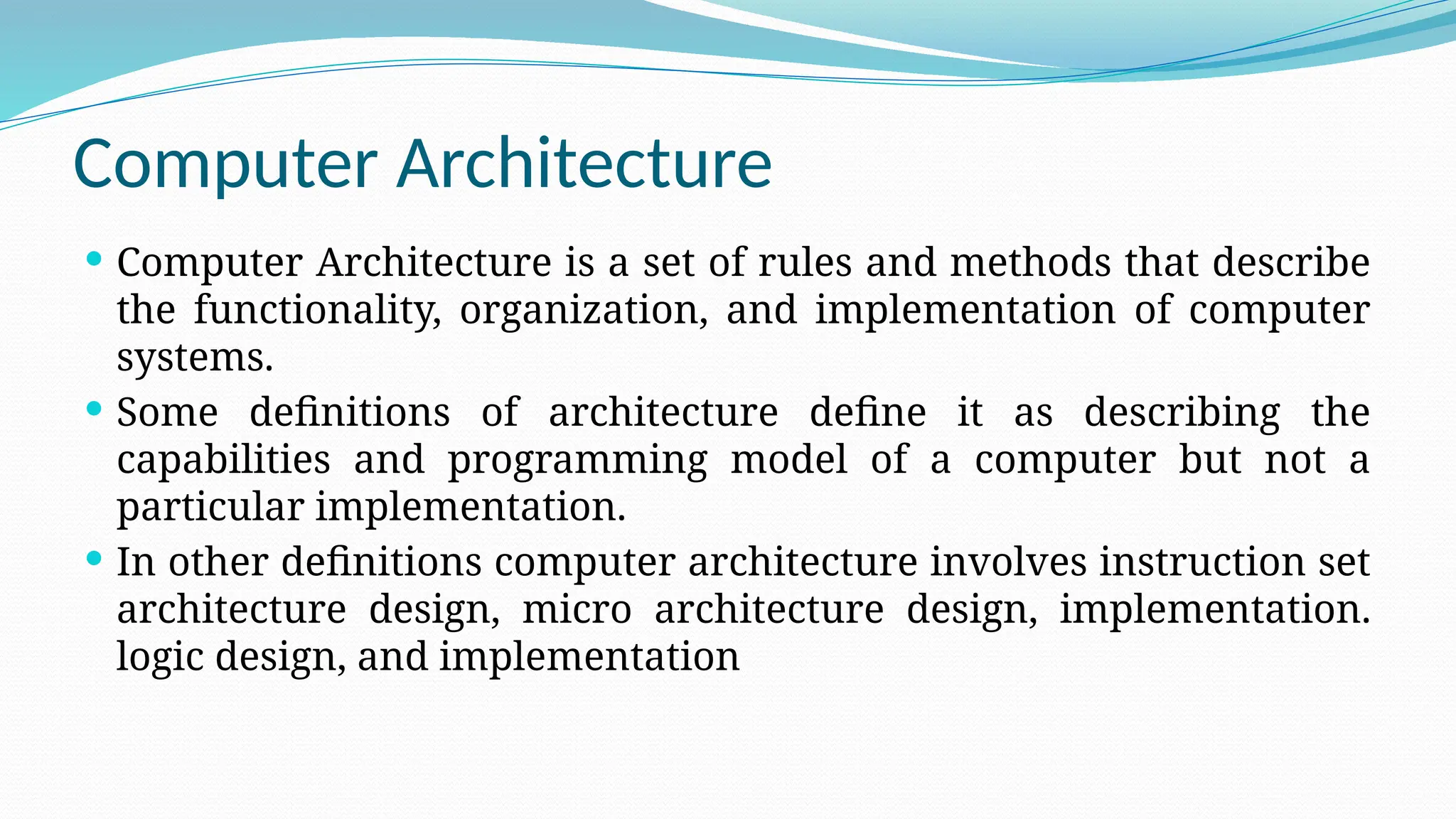
 Computer Architecture is a set of rules and methods that describe
the functionality, organization, and implementation of computer
systems.
 Some definitions of architecture define it as describing the
capabilities and programming model of a computer but not a
particular implementation.
 In other definitions computer architecture involves instruction set
architecture design, micro architecture design, implementation.
logic design, and implementation
Types of computer:
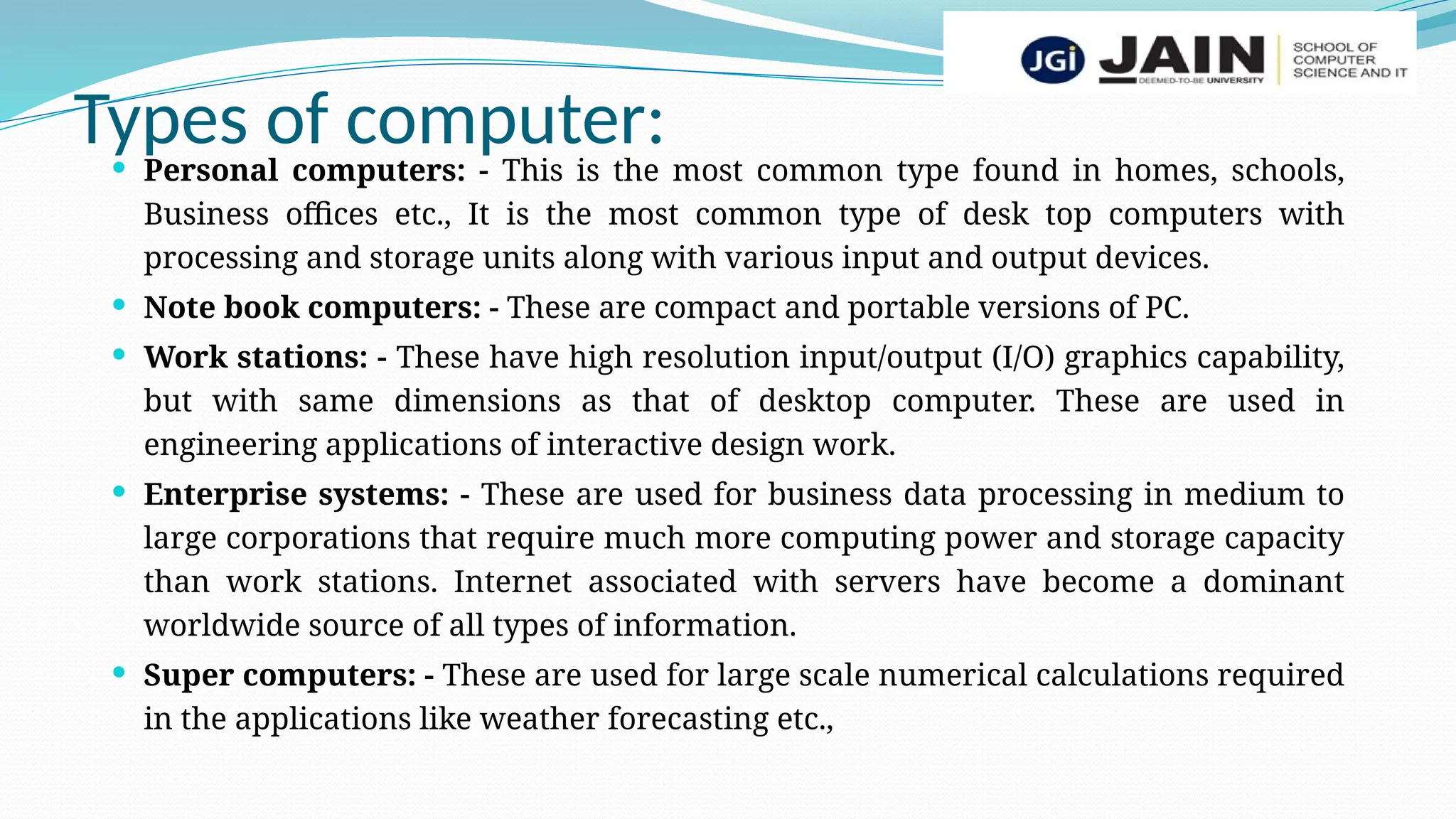
 Personal computers: - This is the most common type found in homes, schools,
Business offices etc., It is the most common type of desk top computers with
processing and storage units along with various input and output devices.
 Note book computers: - These are compact and portable versions of PC.
 Work stations: - These have high resolution input/output (I/O) graphics capability,
but with same dimensions as that of desktop computer. These are used in
engineering applications of interactive design work.
 Enterprise systems: - These are used for business data processing in medium to
large corporations that require much more computing power and storage capacity
than work stations. Internet associated with servers have become a dominant
worldwide source of all types of information.
 Super computers: - These are used for large scale numerical calculations required
in the applications like weather forecasting etc.,
Functional unit
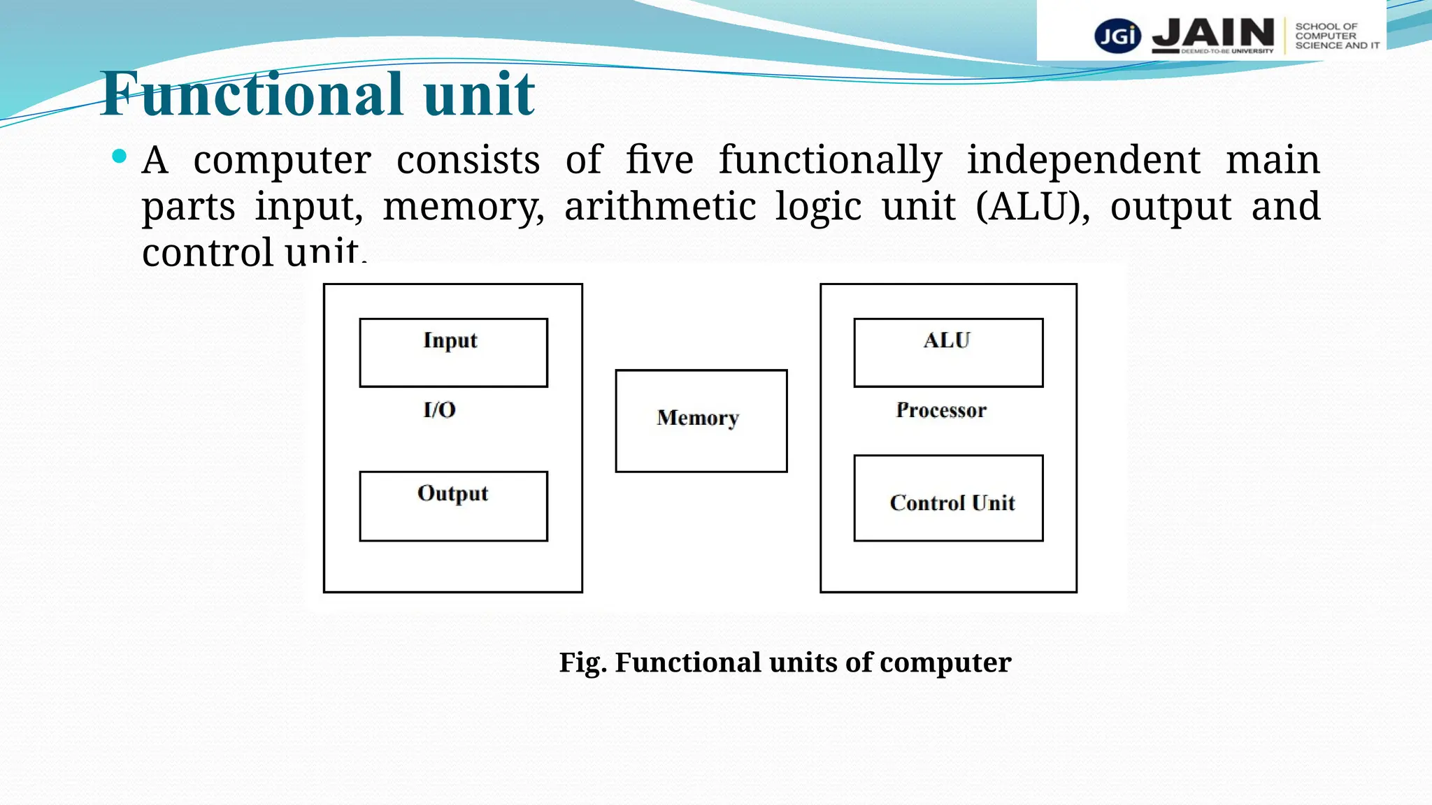
 A computer consists of five functionally independent main
parts input, memory, arithmetic logic unit (ALU), output and
control unit.
Fig. Functional units of computer
 Input device accepts the coded information as source program i.e. high
level language.
 This is either stored in the memory or immediately used by the
processor to perform the desired operations.
 The program stored in the memory determines the processing steps.
Basically the computer converts one source program to an object
program. i.e. into machine language.
 Finally the results are sent to the outside world through output device.
 All of these actions are coordinated by the control unit.
Input Unit
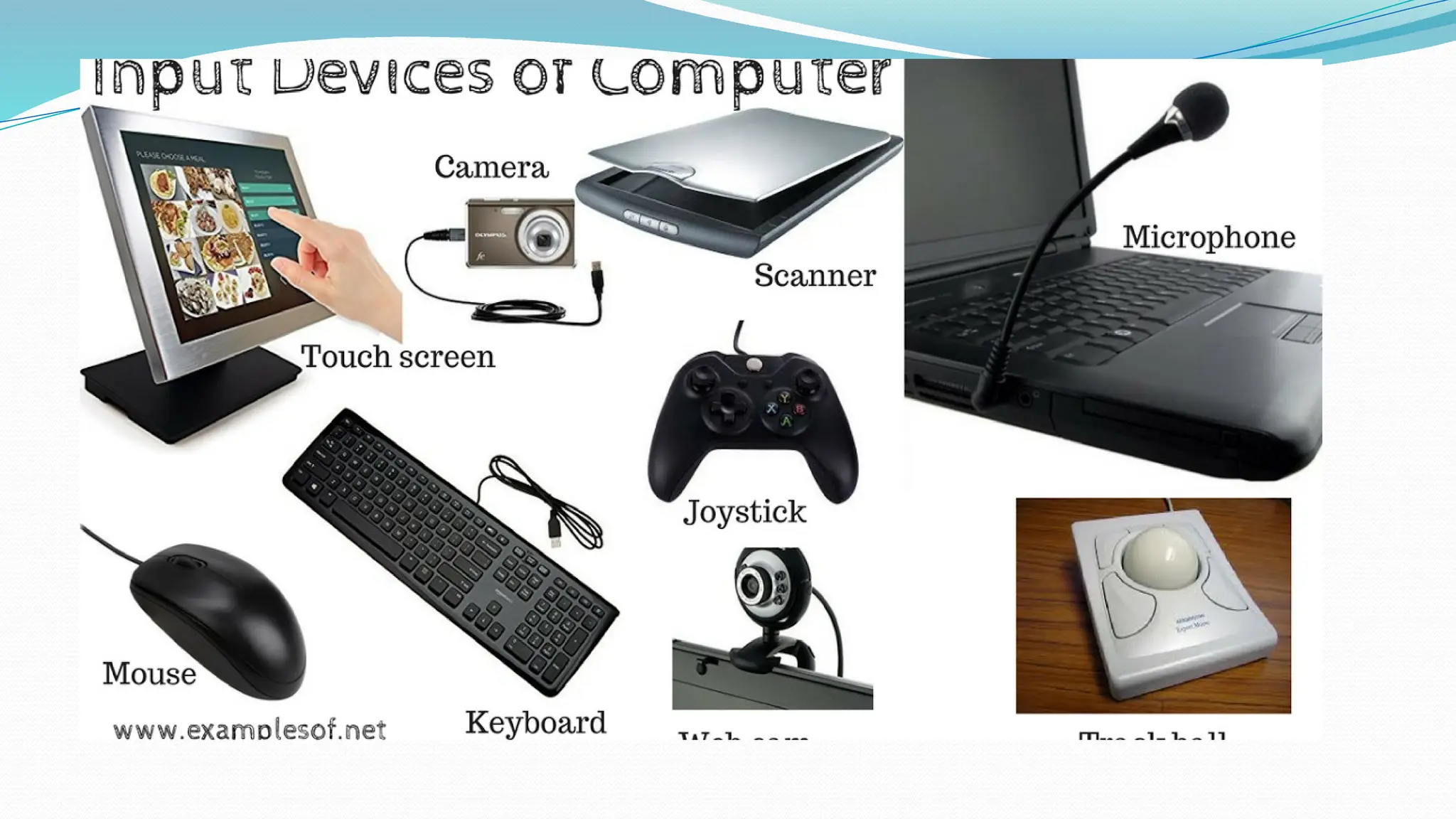
 The source program/high level language program/coded
information/simply data is fed to a computer through input
devices keyboard is a most common type.
 Whenever a key is pressed, one corresponding word or number is
translated into its equivalent binary code over a cable & fed either
to memory or processor.
E.g.
Joysticks, trackballs, mouse, scanners etc are other input devices.
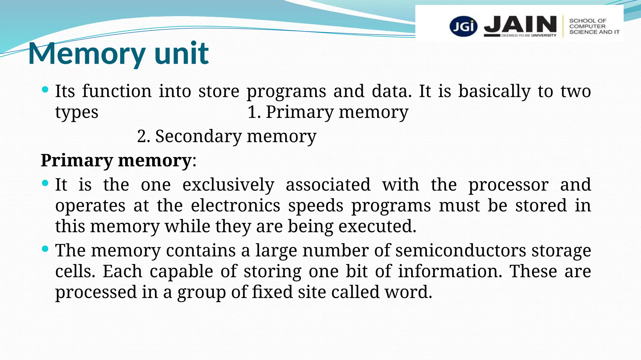
Memory unit
 Its function into store programs and data. It is basically to two
types 1. Primary memory
2. Secondary memory
Primary memory:
 It is the one exclusively associated with the processor and
operates at the electronics speeds programs must be stored in
this memory while they are being executed.
 The memory contains a large number of semiconductors storage
cells. Each capable of storing one bit of information. These are
processed in a group of fixed site called word.
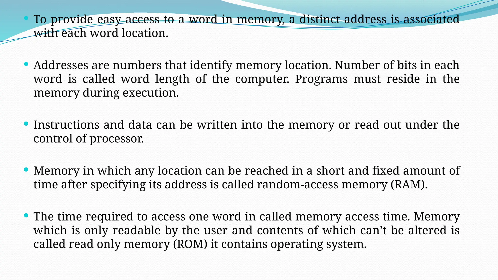
 To provide easy access to a word in memory, a distinct address is associated
with each word location.
 Addresses are numbers that identify memory location. Number of bits in each
word is called word length of the computer. Programs must reside in the
memory during execution.
 Instructions and data can be written into the memory or read out under the
control of processor.
 Memory in which any location can be reached in a short and fixed amount of
time after specifying its address is called random-access memory (RAM).
 The time required to access one word in called memory access time. Memory
which is only readable by the user and contents of which can’t be altered is
called read only memory (ROM) it contains operating system.
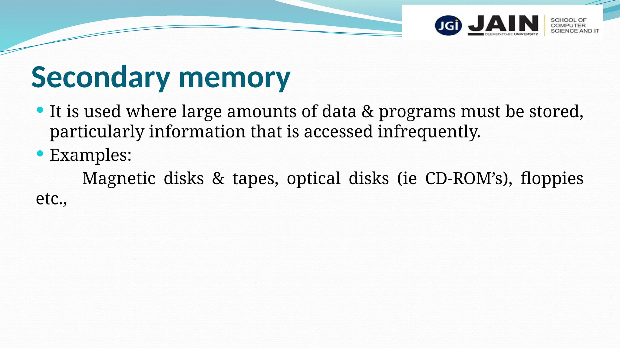
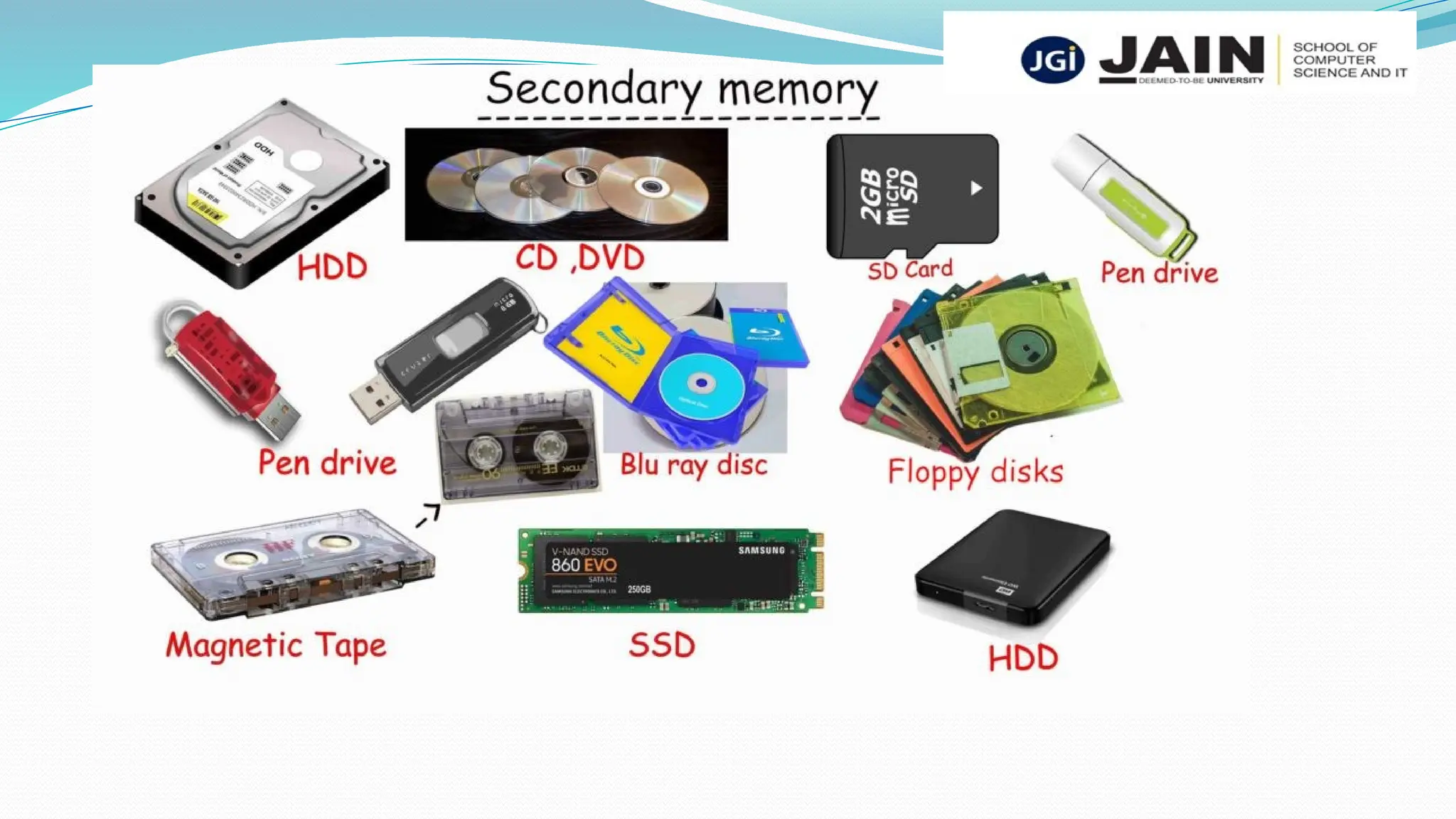
Secondary memory
 It is used where large amounts of data & programs must be stored,
particularly information that is accessed infrequently.
 Examples:
Magnetic disks & tapes, optical disks (ie CD-ROM’s), floppies
etc.,
Arithmetic logic unit (ALU)
 Most of the computer operators are executed in ALU of the
processor like addition, subtraction, division, multiplication, etc.
the operands are brought into the ALU from memory and stored in
high-speed storage elements called register.
 Then according to the instructions, the operation is performed in
the required sequence. The control and the ALU are may times
faster than other devices connected to a computer system.
 This enables a single processor to control a number of external
devices such as keyboards, displays, magnetic and optical disks,
sensors and other mechanical controllers.
Output unit
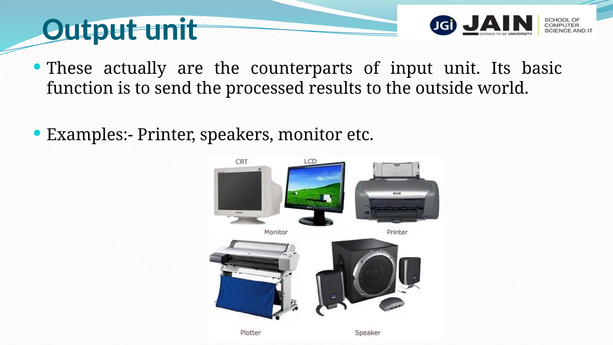
 These actually are the counterparts of input unit. Its basic
function is to send the processed results to the outside world.
 Examples:- Printer, speakers, monitor etc.
Control unit
 It effectively is the nerve center that sends signals to other units
and senses their states.
 The actual timing signals that govern the transfer of data
between input unit, processor, memory and output unit are
generated by the control unit.
17
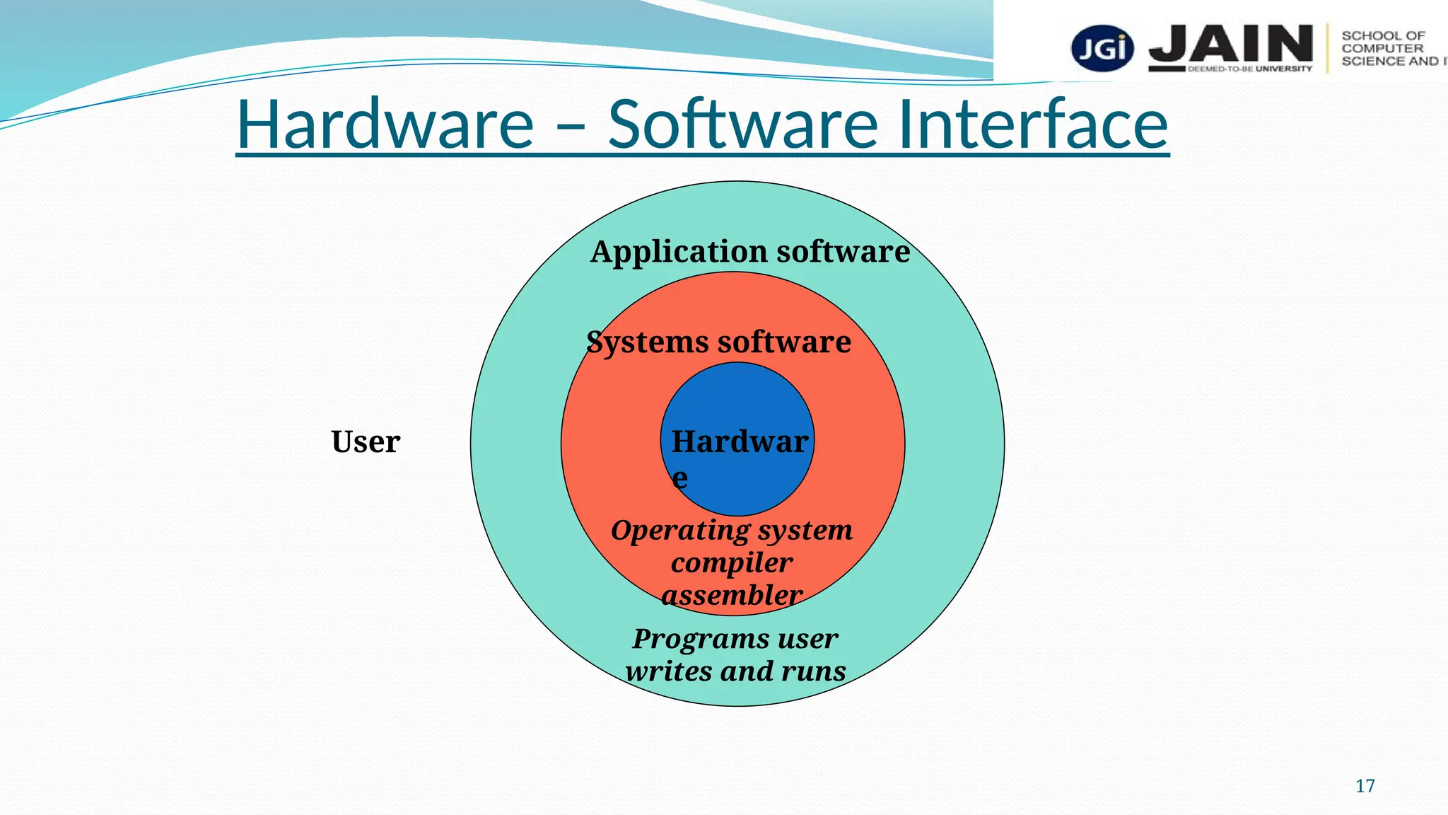
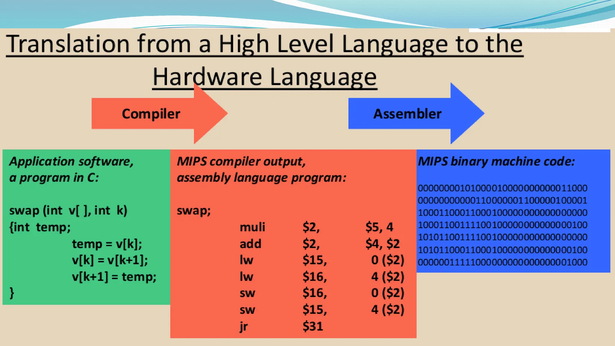
Hardware – Software Interface
Application software
Systems software
Operating system
compiler
assembler
User
Programs user
writes and runs
Hardwar
e
19
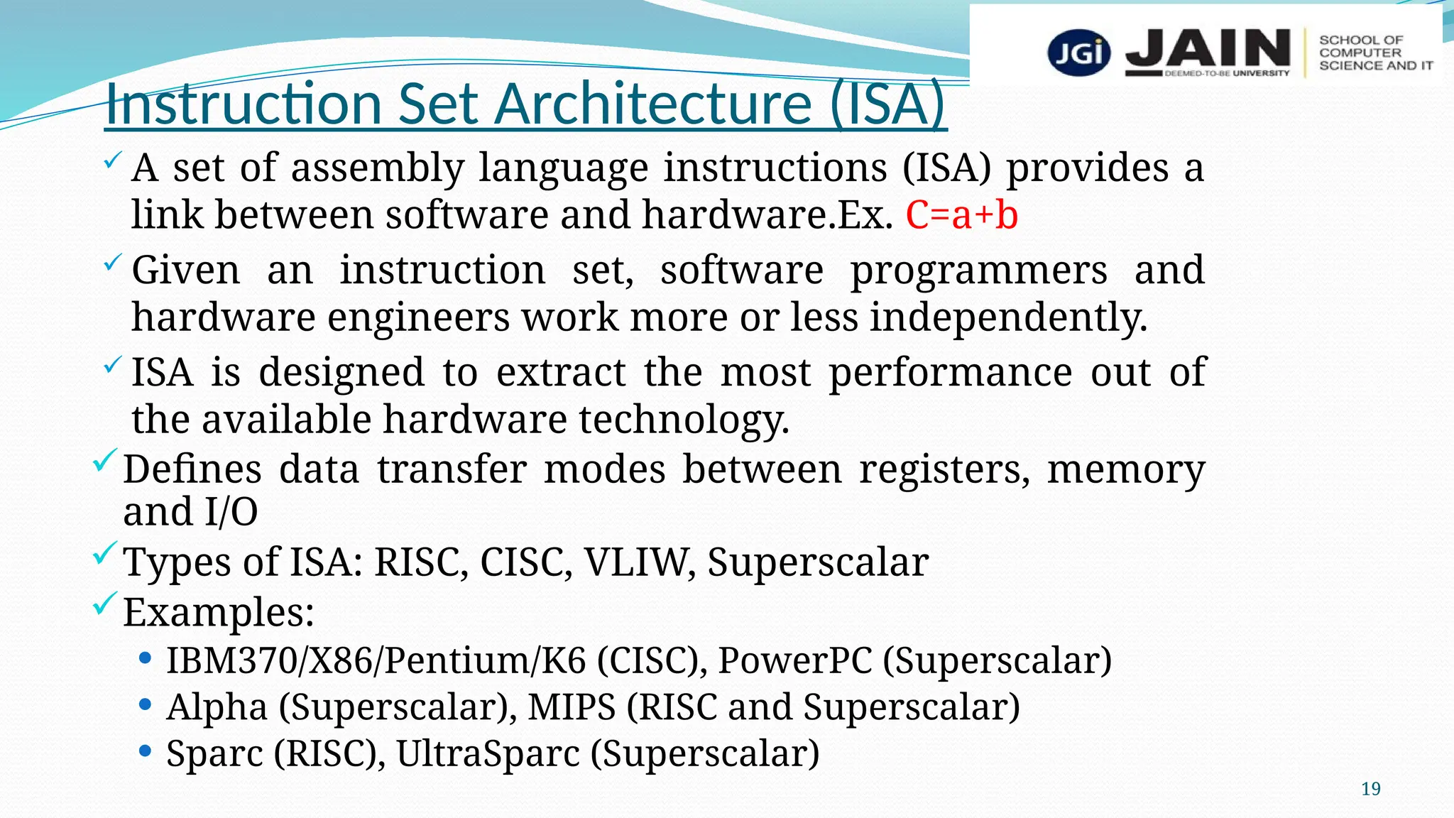
Instruction Set Architecture (ISA)
 A set of assembly language instructions (ISA) provides a
link between software and hardware.Ex. C=a+b
 Given an instruction set, software programmers and
hardware engineers work more or less independently.
 ISA is designed to extract the most performance out of
the available hardware technology.
Defines data transfer modes between registers, memory
and I/O
Types of ISA: RISC, CISC, VLIW, Superscalar
Examples:
 IBM370/X86/Pentium/K6 (CISC), PowerPC (Superscalar)
 Alpha (Superscalar), MIPS (RISC and Superscalar)
 Sparc (RISC), UltraSparc (Superscalar)
20
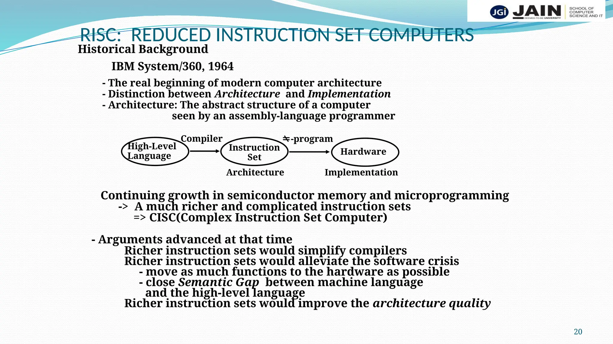
RISC: REDUCED INSTRUCTION SET COMPUTERS
Historical Background
IBM System/360, 1964
- The real beginning of modern computer architecture
- Distinction between Architecture and Implementation
- Architecture: The abstract structure of a computer
seen by an assembly-language programmer
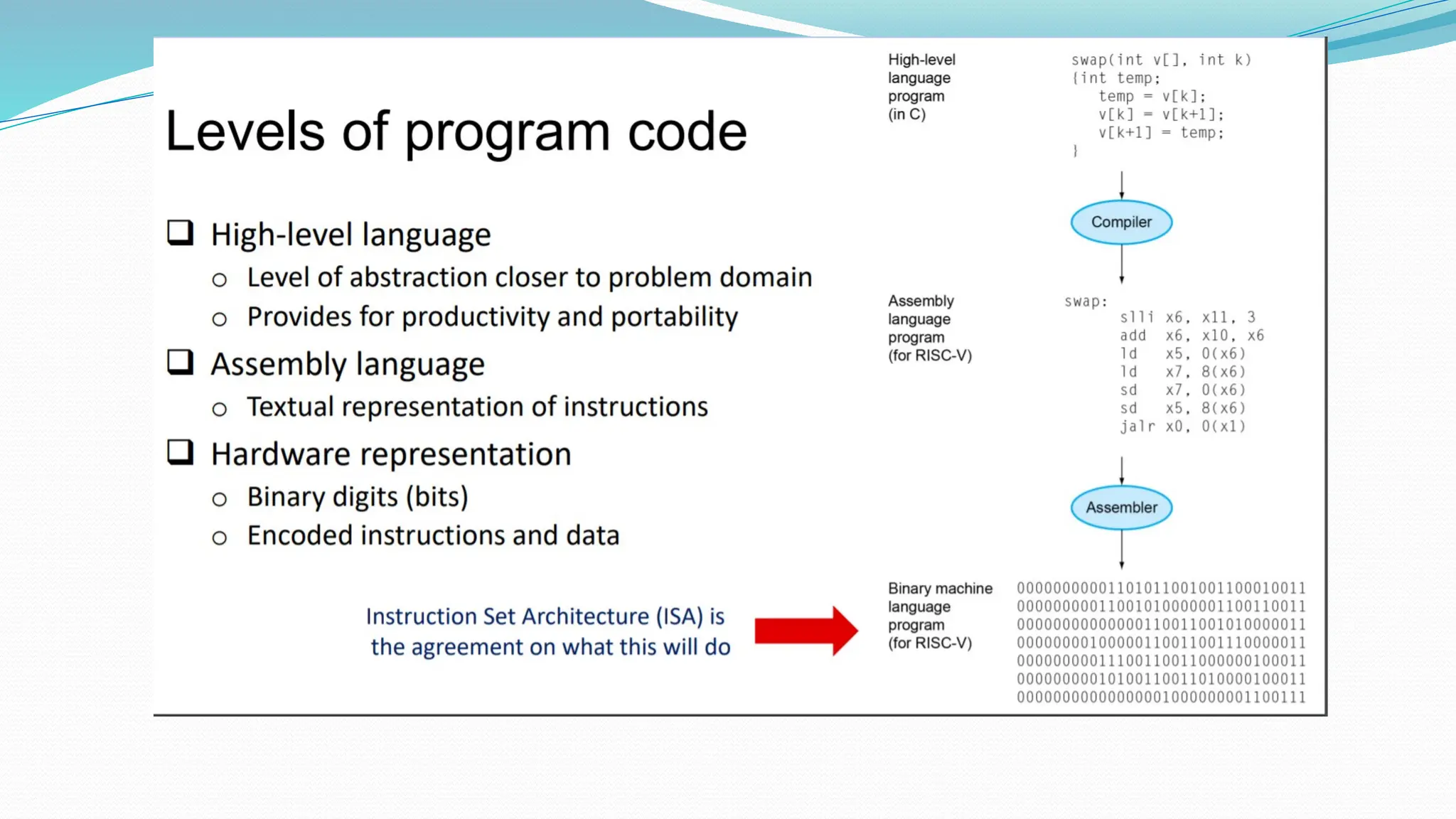
High-Level
Language
Instruction
Set
Hardware
Compiler -program
Architecture Implementation
Continuing growth in semiconductor memory and microprogramming
-> A much richer and complicated instruction sets
=> CISC(Complex Instruction Set Computer)
- Arguments advanced at that time
Richer instruction sets would simplify compilers
Richer instruction sets would alleviate the software crisis
- move as much functions to the hardware as possible
- close Semantic Gap between machine language
and the high-level language
Richer instruction sets would improve the architecture quality
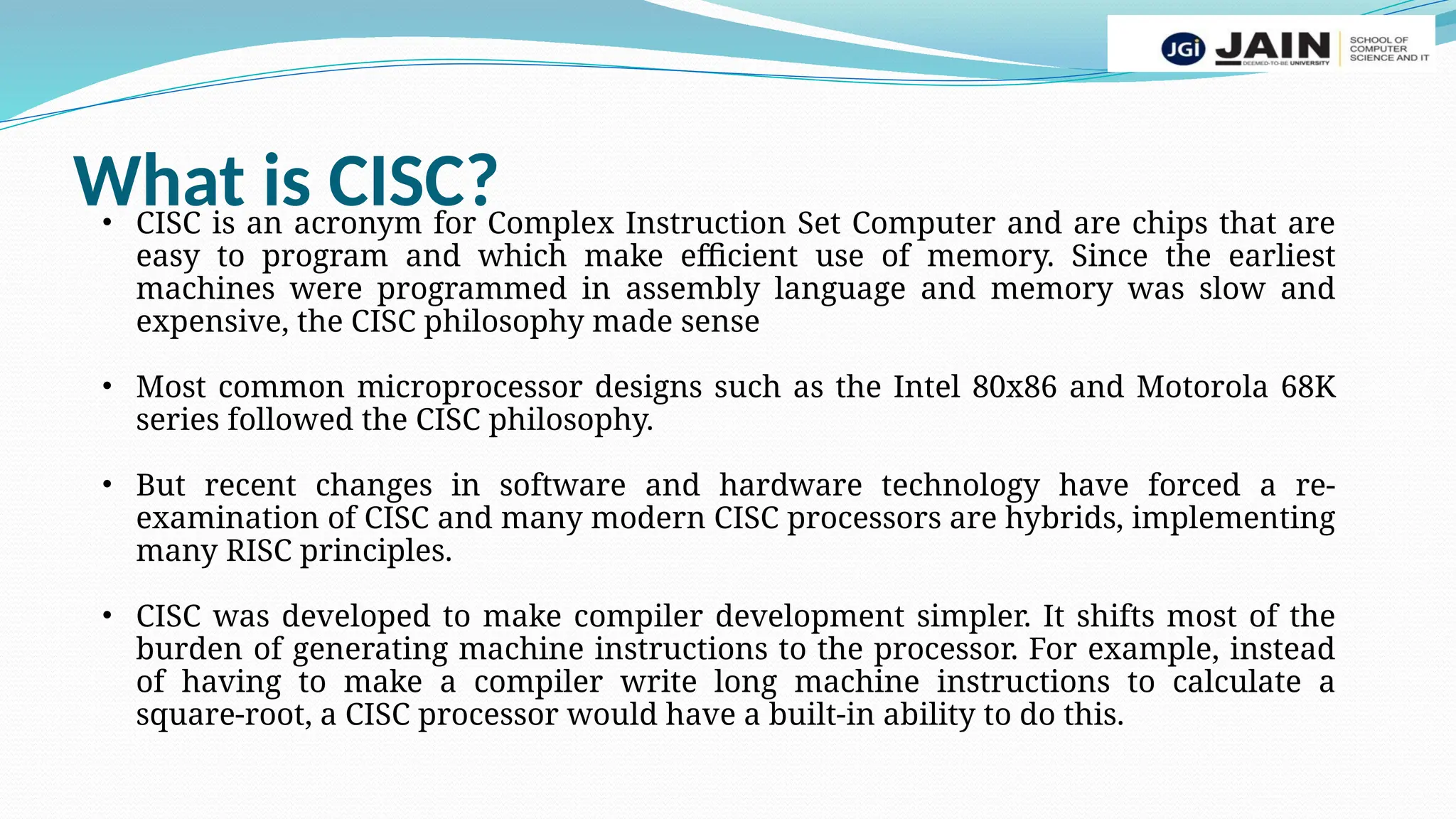
What is CISC?
• CISC is an acronym for Complex Instruction Set Computer and are chips that are
easy to program and which make efficient use of memory. Since the earliest
machines were programmed in assembly language and memory was slow and
expensive, the CISC philosophy made sense
• Most common microprocessor designs such as the Intel 80x86 and Motorola 68K
series followed the CISC philosophy.
• But recent changes in software and hardware technology have forced a re-
examination of CISC and many modern CISC processors are hybrids, implementing
many RISC principles.
• CISC was developed to make compiler development simpler. It shifts most of the
burden of generating machine instructions to the processor. For example, instead
of having to make a compiler write long machine instructions to calculate a
square-root, a CISC processor would have a built-in ability to do this.
22
COMPLEX INSTRUCTION SET COMPUTERS: CISC
High Performance General Purpose Instructions
Characteristics of CISC:
1. A large number of instructions (from 100-250 usually)
2. Some instructions that performs a certain tasks are not used
frequently.
3. Many addressing modes are used (5 to 20)
4. Variable length instruction format.
5. Instructions that manipulate operands in memory.
1. C=a+b
2. Ex: ADD A B
23
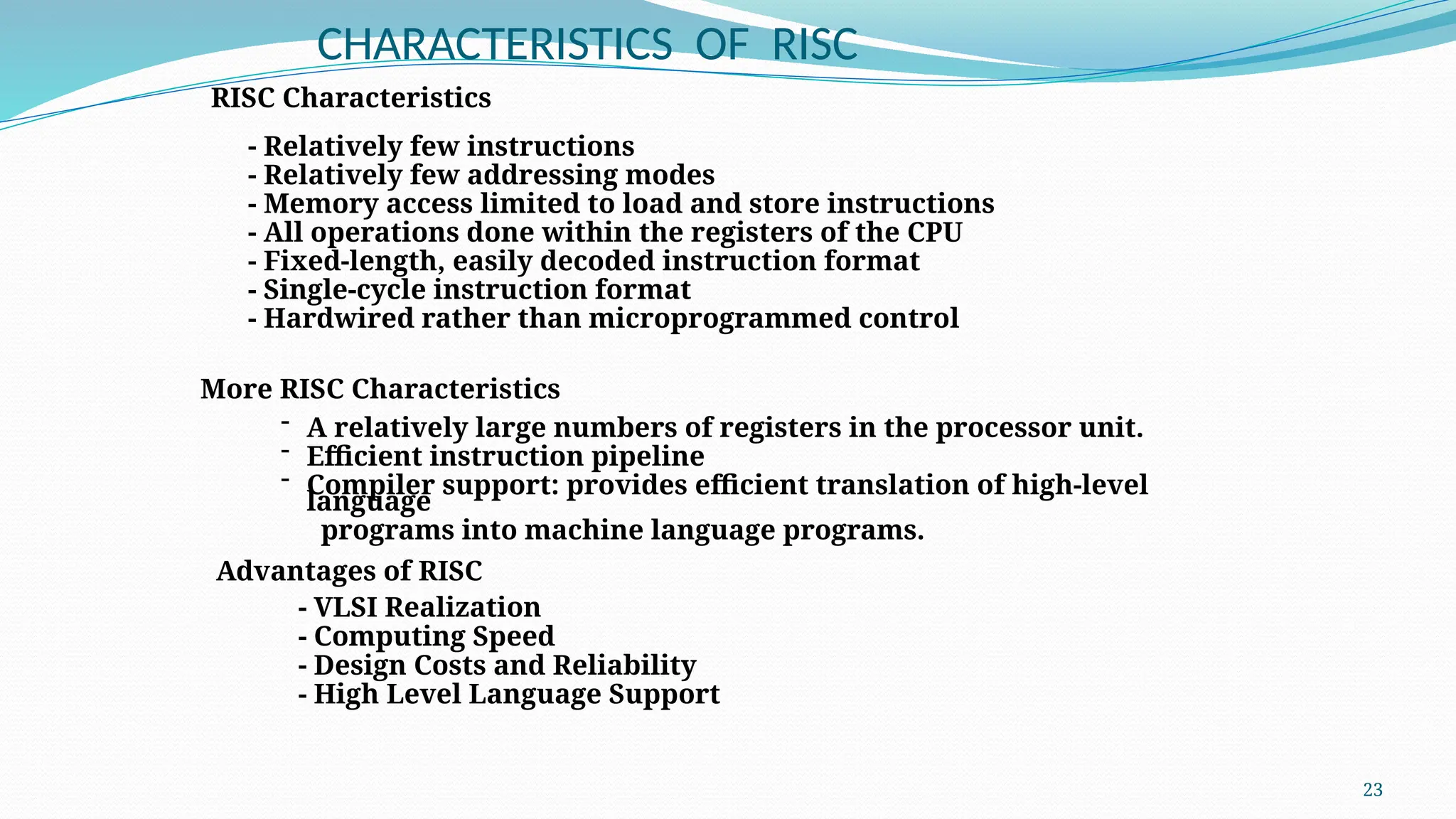
CHARACTERISTICS OF RISC
RISC Characteristics
- Relatively few instructions
- Relatively few addressing modes
- Memory access limited to load and store instructions
- All operations done within the registers of the CPU
- Fixed-length, easily decoded instruction format
- Single-cycle instruction format
- Hardwired rather than microprogrammed control
- A relatively large numbers of registers in the processor unit.
- Efficient instruction pipeline
- Compiler support: provides efficient translation of high-level
language
programs into machine language programs.
More RISC Characteristics
Advantages of RISC
- VLSI Realization
- Computing Speed
- Design Costs and Reliability
- High Level Language Support
24
Contd.
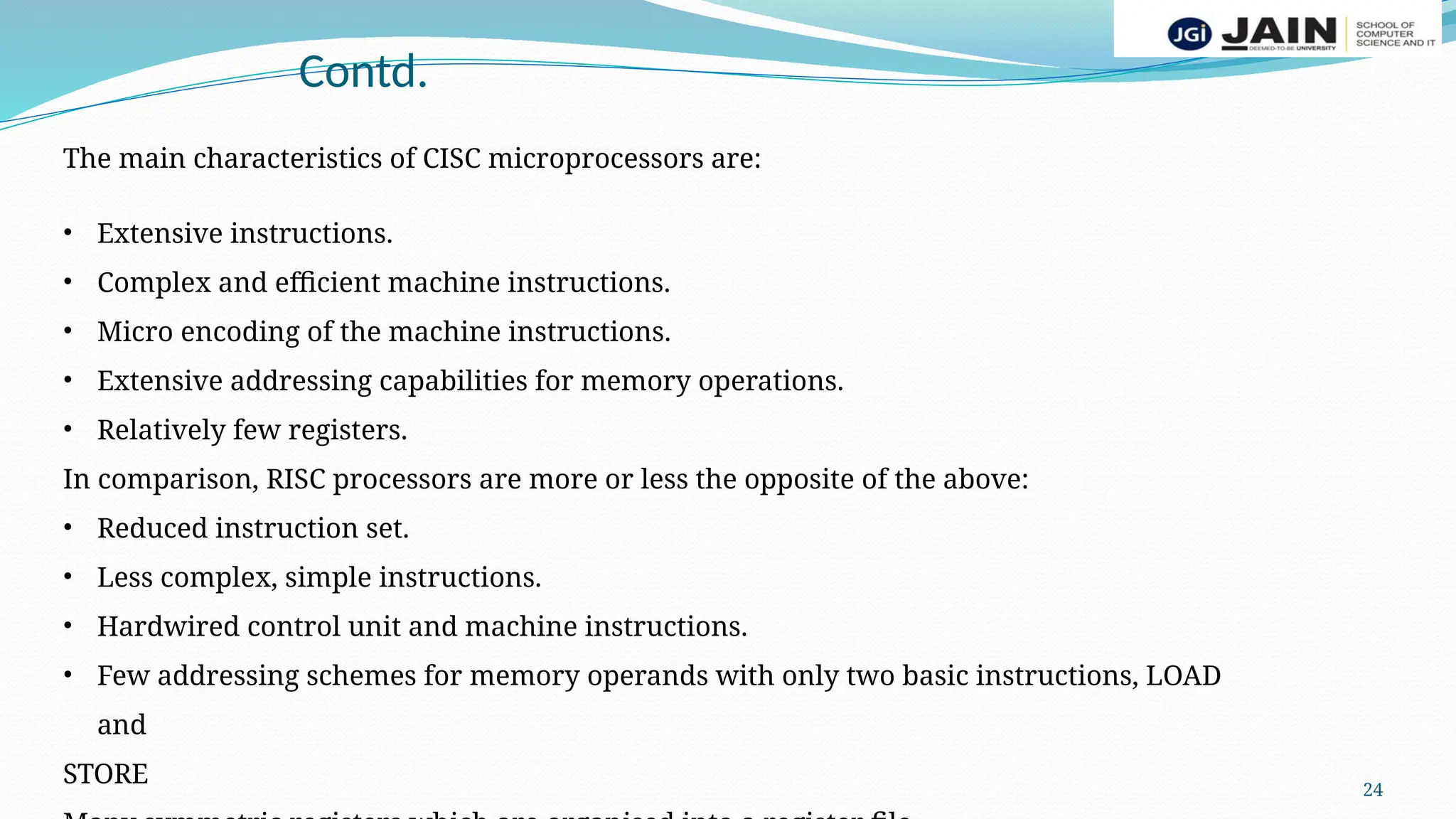
The main characteristics of CISC microprocessors are:
• Extensive instructions.
• Complex and efficient machine instructions.
• Micro encoding of the machine instructions.
• Extensive addressing capabilities for memory operations.
• Relatively few registers.
In comparison, RISC processors are more or less the opposite of the above:
• Reduced instruction set.
• Less complex, simple instructions.
• Hardwired control unit and machine instructions.
• Few addressing schemes for memory operands with only two basic instructions, LOAD
and
STORE
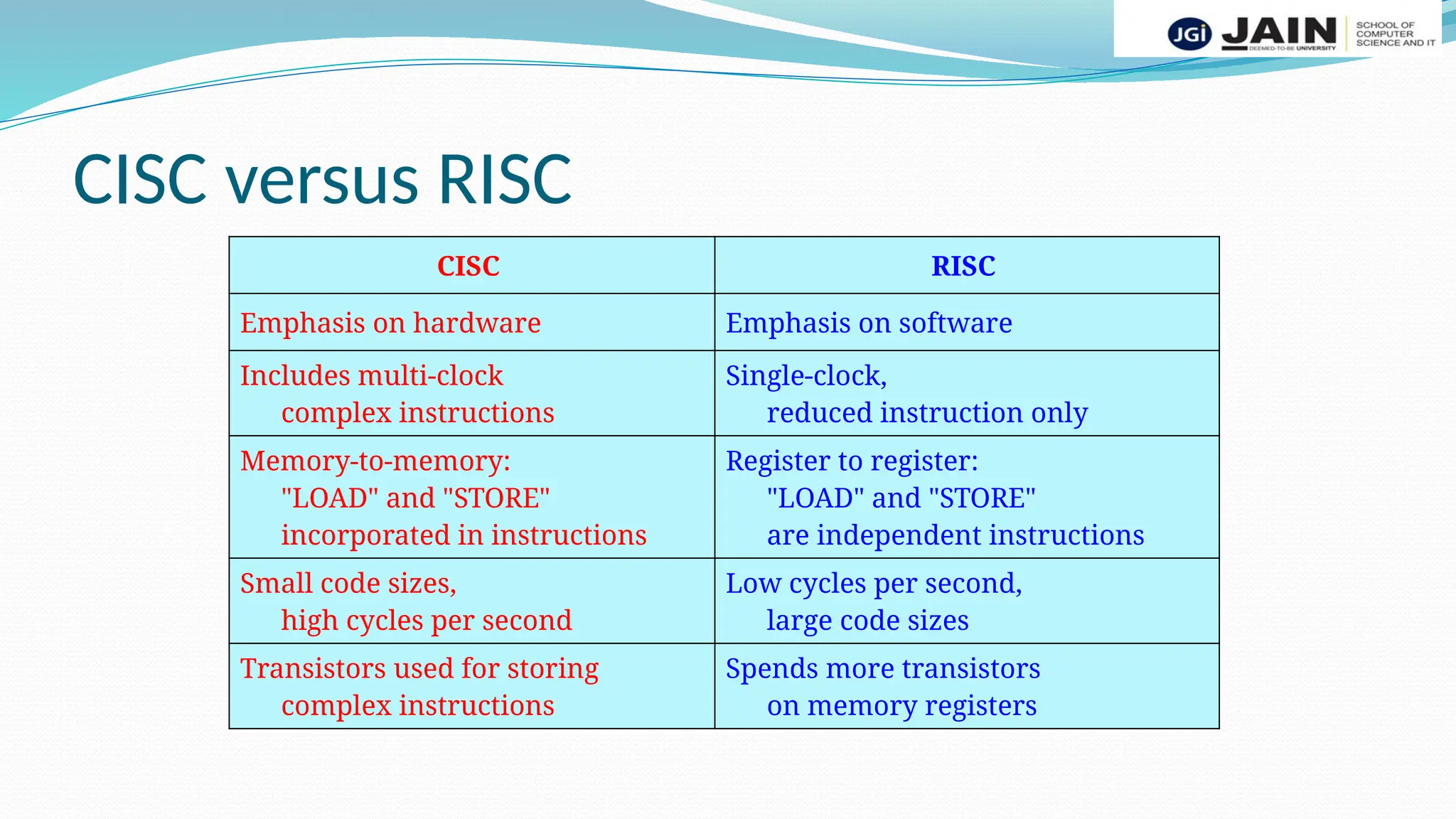
CISC versus RISC
CISC RISC
Emphasis on hardware Emphasis on software
Includes multi-clock
complex instructions
Single-clock,
reduced instruction only
Memory-to-memory:
"LOAD" and "STORE"
incorporated in instructions
Register to register:
"LOAD" and "STORE"
are independent instructions
Small code sizes,
high cycles per second
Low cycles per second,
large code sizes
Transistors used for storing
complex instructions
Spends more transistors
on memory registers
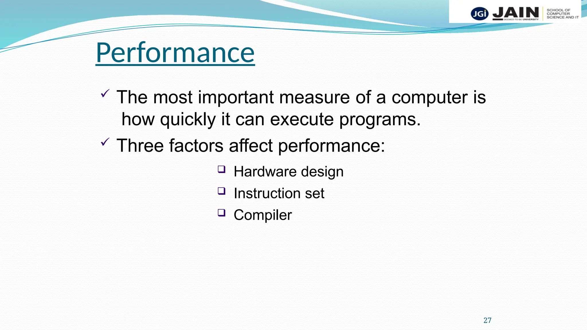
 The most important measure of a computer is
how quickly it can execute programs.
 Three factors affect performance:
 Hardware design
 Instruction set
 Compiler
Performance
27
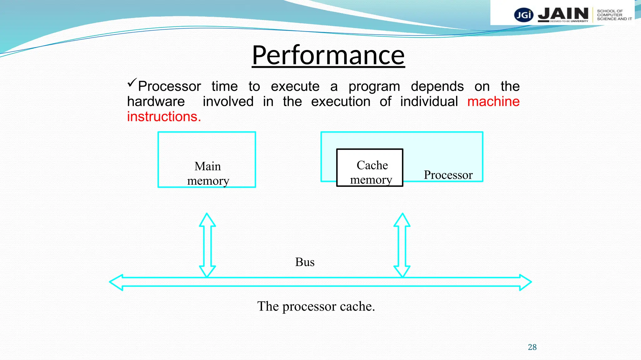
Processor time to execute a program depends on the
hardware involved in the execution of individual machine
instructions.
Main
memory Processor
Bus
Cache
memory
The processor cache.
Performance
28
 The processor and a relatively small cache
memory can be fabricated on a single
integrated circuit chip.
 Speed
 Cost
 Memory management
Performance
29
Processor
Clock
30
 Clock, clock cycle, and clock rate
 The execution of each instruction is divided
into several steps, each of which
completes in one clock cycle.
 Hertz – cycles per second
Basic Performance Equation
31
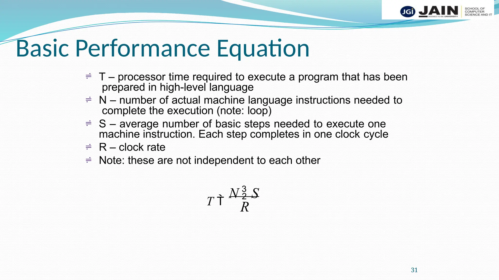
 T – processor time required to execute a program that has been
prepared in high-level language
N – number of actual machine language instructions needed to
complete the execution (note: loop)
S – average number of basic steps needed to execute one
machine instruction. Each step completes in one clock cycle
R – clock rate
Note: these are not independent to each other
T 
N  S




R
Clock Rate
32
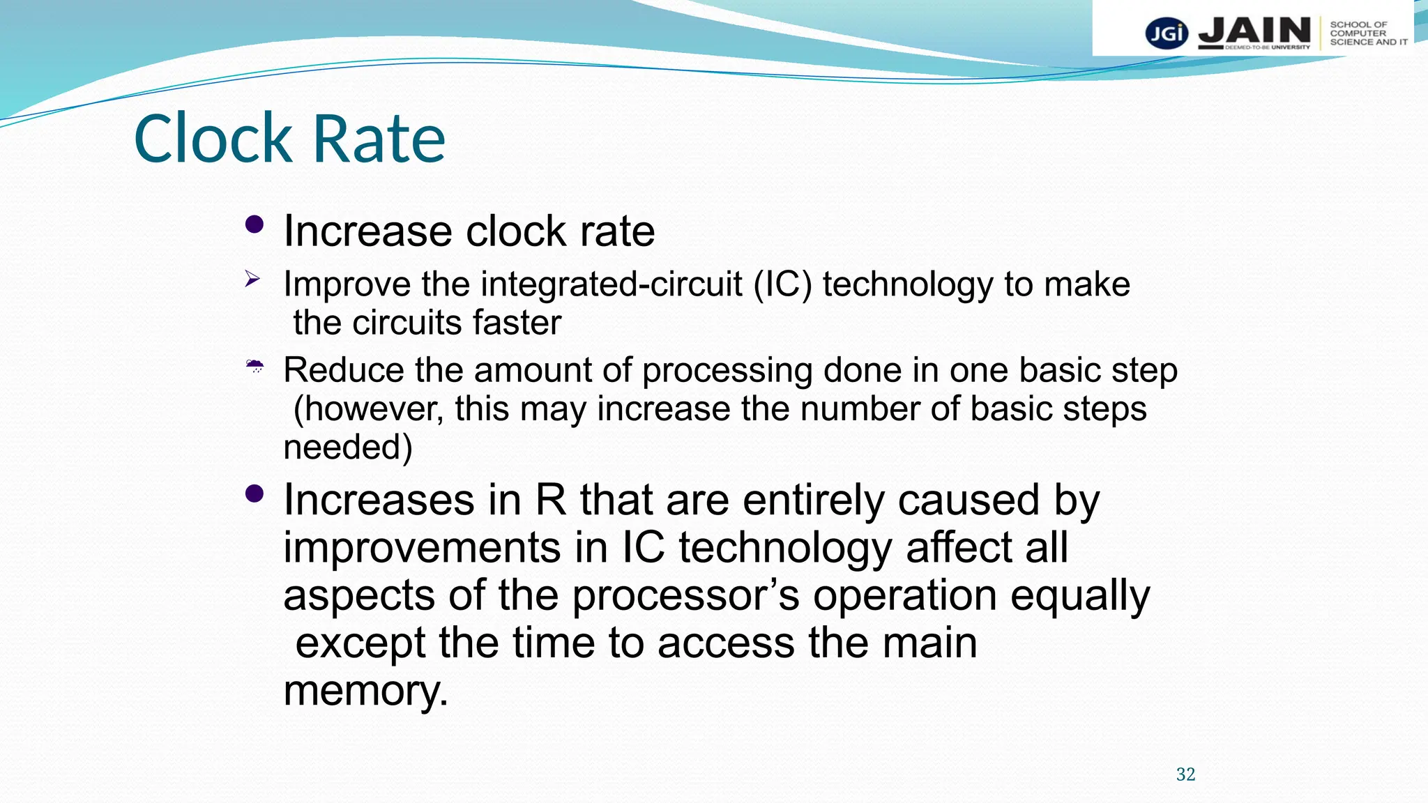
 Increase clock rate

 Improve the integrated-circuit (IC) technology to make
the circuits faster
Reduce the amount of processing done in one basic step
(however, this may increase the number of basic steps
needed)
 Increases in R that are entirely caused by
improvements in IC technology affect all
aspects of the processor’s operation equally
except the time to access the main
memory.
Compiler
33
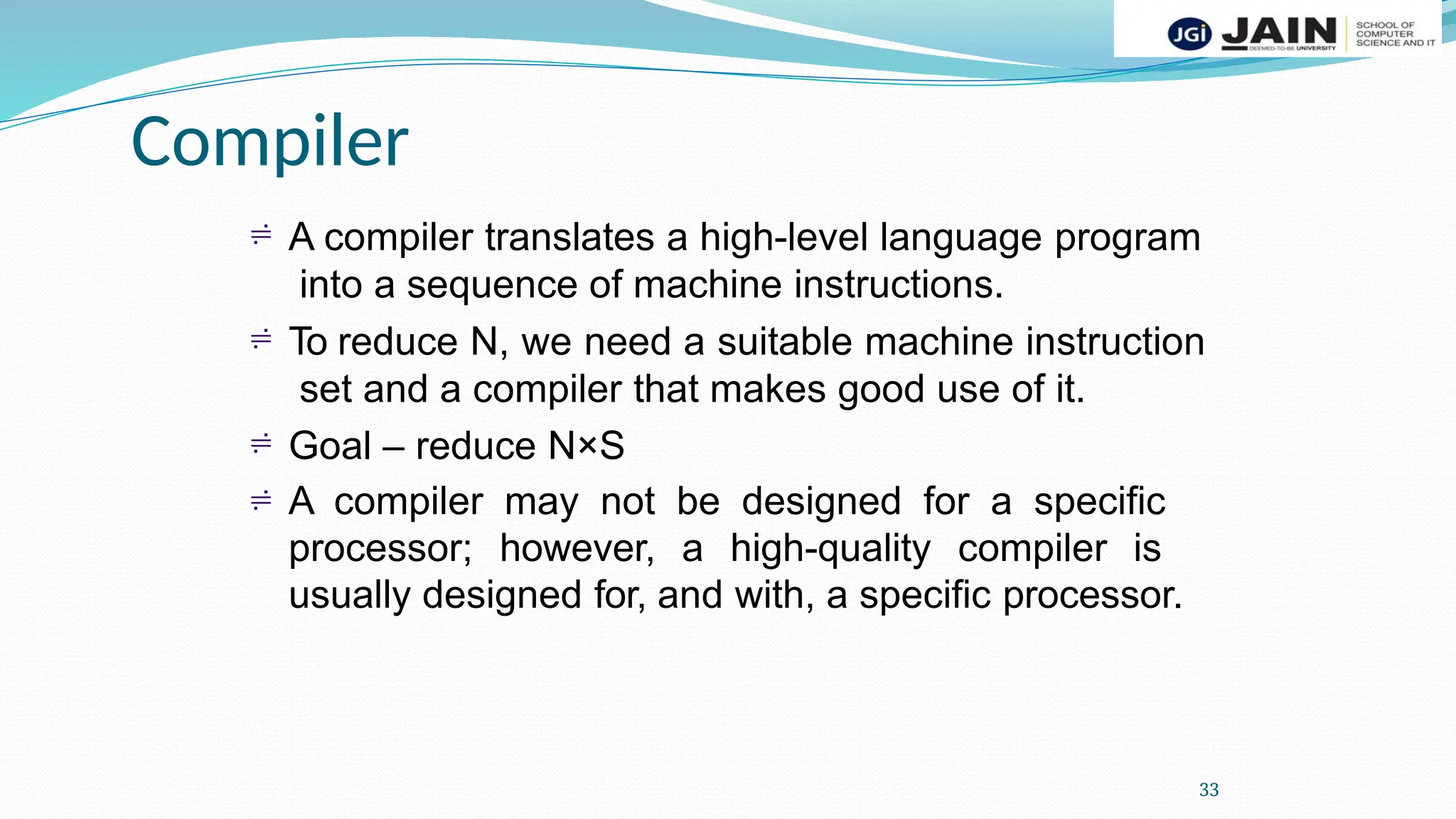
 A compiler translates a high-level language program
into a sequence of machine instructions.
To reduce N, we need a suitable machine instruction
set and a compiler that makes good use of it.
Goal – reduce N×S
A compiler may not be designed for a specific
processor; however, a high-quality compiler is
usually designed for, and with, a specific processor.



Performance Measurement
34



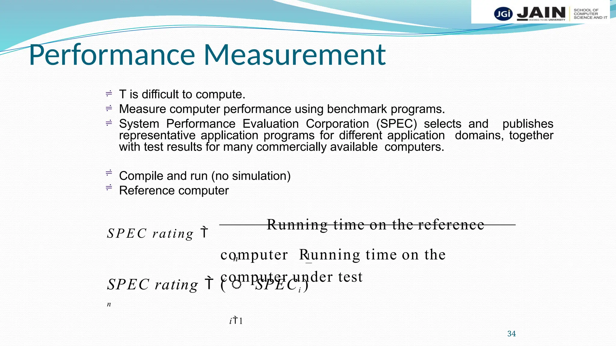
T is difficult to compute.
Measure computer performance using benchmark programs.
System Performance Evaluation Corporation (SPEC) selects and publishes
representative application programs for different application domains, together
with test results for many commercially available computers.
Compile and run (no simulation)
Reference computer


S P E C rating 
Running time on the reference
computer Running time on the
computer under test
n 1
SPEC rating  ( SPECi )
n
i1
Amdahl's Law
Amdahl's law states that performance improvement to be gained by using a
faster mode of execution is limited by the fraction of time the faster mode can
be used. Using this law, the performance gain that can be obtained by
improving some portion of the computer can be calculated using the following
formula.
Performance
of entire task using the enhancement when possible
Speedup = ---------------------------------------------------------
Performance for the entire task without using the enhancement
BUS STRUCTURES
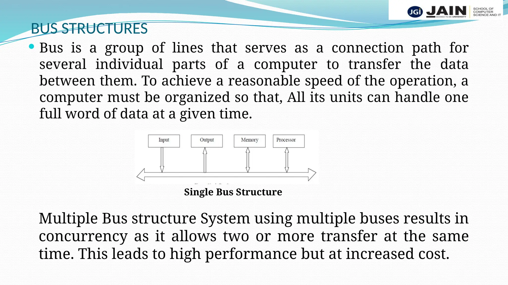
 Bus is a group of lines that serves as a connection path for
several individual parts of a computer to transfer the data
between them. To achieve a reasonable speed of the operation, a
computer must be organized so that, All its units can handle one
full word of data at a given time.
Single Bus Structure
Multiple Bus structure System using multiple buses results in
concurrency as it allows two or more transfer at the same
time. This leads to high performance but at increased cost.
INSTRUCTION AND INSTRUCTION SEQUENCING
 A computer must have instruction capable of performing four
types of basic operations such as Data transfer between the
memory and the processor registers.
 Arithmetic and logic operation on data Program sequencing and
control I/O transfers To understand the first two types of
instruction, we need to know some notations.
 Register Transfer Notation
 Assembly Language Notation
Register Transfer Notation (RTN)
 Data transfer can be represented by standard notations given below.
 Processor registers are represented by notations R0, R1, R2.
 Address of the memory locations are represented by names such as LOC, PLACE,
MEM etc..
 I/O registers are represented by names such as DATAIN, DATAOUT.
 The content of memory locations are denoted by placing square bracket around the
name of the register.
 Example 1: R1 [LOC]
←
 This expression states that the contents of memory location LOC are transferred into the
processor register R1.
 Example 2: R3 [R1] + [R2]
←
 This expression states that the contents of processor registers R1 and R2 are added and
the result is stored into the processor register R3. This type of notation is known as
Register Transfer Notation (RTN).
Assembly Language Notation
 To represent machine instructions, assembly language uses
statements as shown below To transfer the data from memory
location LOC to processor register R1
 Move LOC, R1 ( Syntax: MOVE LOCATION, REGISTER)
 To add two numbers in register R1 and R2 and to place their sum in
register R3
 ADD R1, R2, R3 (: R3 [R1] + [R2]
← )
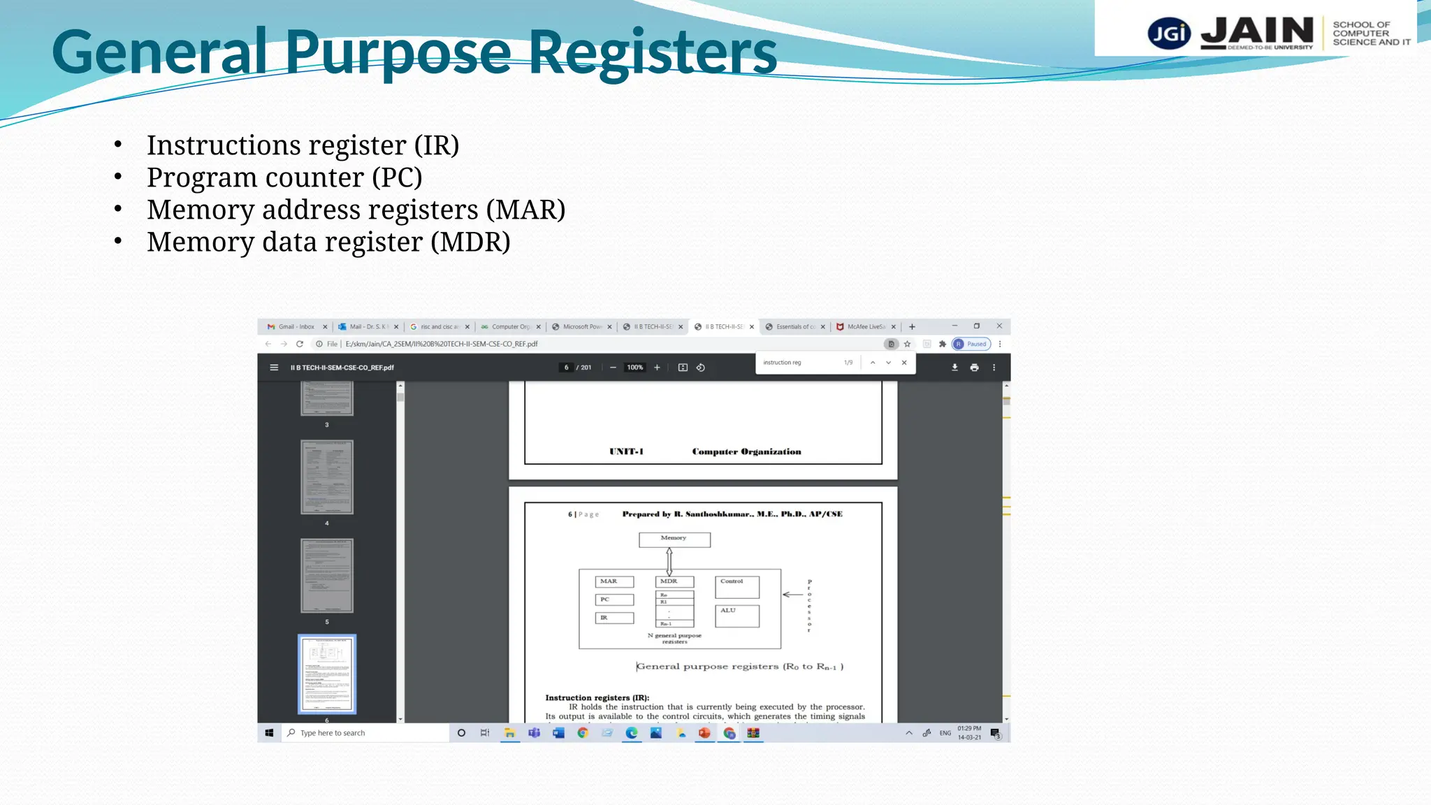
General Purpose Registers
• Instructions register (IR)
• Program counter (PC)
• Memory address registers (MAR)
• Memory data register (MDR)
 Instruction registers (IR): IR holds the instruction that is currently
being executed by the processor. Its output is available to the control
circuits, which generates the timing signals that controls various
processing elements involved in executing the instruction.
 Program counter (PC): It is a special purpose register that contains
the address of the next instruction to be fetched and executed.
During the execution of one instruction PC is updated to point the
address of the next instruction to be fetched and executed. It keeps
track of the execution of a program.
 Memory address registers (MAR): The MAR holds the address of
the memory location to be accessed.
 Memory data register (MDR): The MDR contains the data to be
written into or read from the memory location that is being pointed
by MAR. These two registers MAR and MDR facilitates
communication between memory and the processor.
Buffer registers
 Buffer register is an electronic register that is included with the
devices to hold the information during transfer. When the processor
sends a set of characters to a printer, those contents is transferred to
the printer buffer (buffer register for a printer). Once printer buffer
is loaded processor and the bus is no longer needed and the
processor can be released for other activity.
 Purpose of Buffer Register:
✓ Buffer register prevent a high speed processor from being
locked to a slow I/O devices.
✓ Buffer register is used which smooth out timing differences
among slow and the fast devices.
✓ It allows the processor to switch rapidly from one device to
another.
ISA
 Interface between the high level language and the
machine language It has the following parts:
 Instruction set
Addressing modes
 Instruction formats
 Instruction representation
Instructions
Logical instructions
 AND, OR, XOR, Shift
Arithmetic instructions
Data types
Integers: Unsigned, Signed, Byte, Short, Long
Real numbers: Single precision (float), Double precision (double)
Operations
Addition, Subtraction, Multiplication, Division
Data transfer instructions
Register transfer: Move
Memory transfer: Load, Store
I/O transfer: In, Out
Control transfer instructions
• Unconditional branch
• Conditional branch
• Procedure call
• Return
45
INSTRUCTION FORMAT
OP-code field - specifies the operation to be performed
Address field - designates memory address(s) or a processor register(s)
Mode field - specifies the way the operand or the
effective address is determined
The number of address fields in the instruction format
depends on the internal organization of CPU
- The three most common CPU organizations:
Single accumulator organization:
ADD X /* AC  AC + M[X] */
General register organization:
ADD R1, R2, R3 /* R1  R2 + R3 */
ADD R1, R2 /* R1  R1 + R2 */
MOV R1, R2 /* R1  R2 */
ADD R1, X /* R1  R1 + M[X] */
Stack organization:
PUSH X /* TOS  M[X] */
ADD
Instruction Fields
46
THREE, and TWO-ADDRESS
INSTRUCTIONS
Three-Address Instructions:
Program to evaluate X = (A + B) * (C + D) :
ADD R1, A, B /* R1  M[A] + M[B] */
ADD R2, C, D /* R2  M[C] + M[D] */
MUL X, R1, R2 /* M[X]  R1 * R2 */
- Results in short programs
- Instruction becomes long (many bits)
Two-Address Instructions:
Program to evaluate X = (A + B) * (C + D) :
MOV R1, A /* R1  M[A] */
ADD R1, B /* R1  R1 + M[B] */
MOV R2, C /* R2  M[C] */
ADD R2, D /* R2  R2 + M[D] */
MUL R1, R2 /* R1  R1 * R2 */
MOV X, R1 /* M[X]  R1 */
47
ONE, and ZERO-ADDRESS INSTRUCTIONS
One-Address Instructions:
- Use an implied AC register for all data manipulation
- Program to evaluate X = (A + B) * (C + D) :
LOAD A /* AC  M[A] */
ADD B /* AC  AC + M[B] */
STORE T /* M[T]  AC */
LOAD C /* AC  M[C] */
ADD D /* AC  AC + M[D] */
MUL T /* AC  AC * M[T]*/
STORE X /* M[X]  AC */
Zero-Address Instructions:
- Can be found in a stack-organized computer
- Program to evaluate X = (A + B) * (C + D) :
PUSH A /* TOS  A */
PUSH B /* TOS  B */
ADD /* TOS  (A + B) */
PUSH C /* TOS  C */
PUSH D /* TOS  D */
ADD /* TOS  (C + D) */
MUL /* TOS  (C + D) * (A + B) */
POP X /* M[X]  TOS */
 Complex Instruction Set Computer (CISC) processors:
2 operand instructions and 1 operand instructions
Any instruction can use memory operands, Many addressing
modes, Complex instruction formats: Varying length instructions ,
Micro programmed control unit.
Reduced Instruction Set Computer (RISC) processors:
3 operand instructions, 2 operand instructions, and 1 operand
instructions. Architecture processors:
• Only memory transfer instructions (Load and Store) can use
memory operands.
• All other instructions can use register operands only.
– A few addressing modes.
– Simple instruction formats: Fixed length instructions.
– Hardwired control unit.
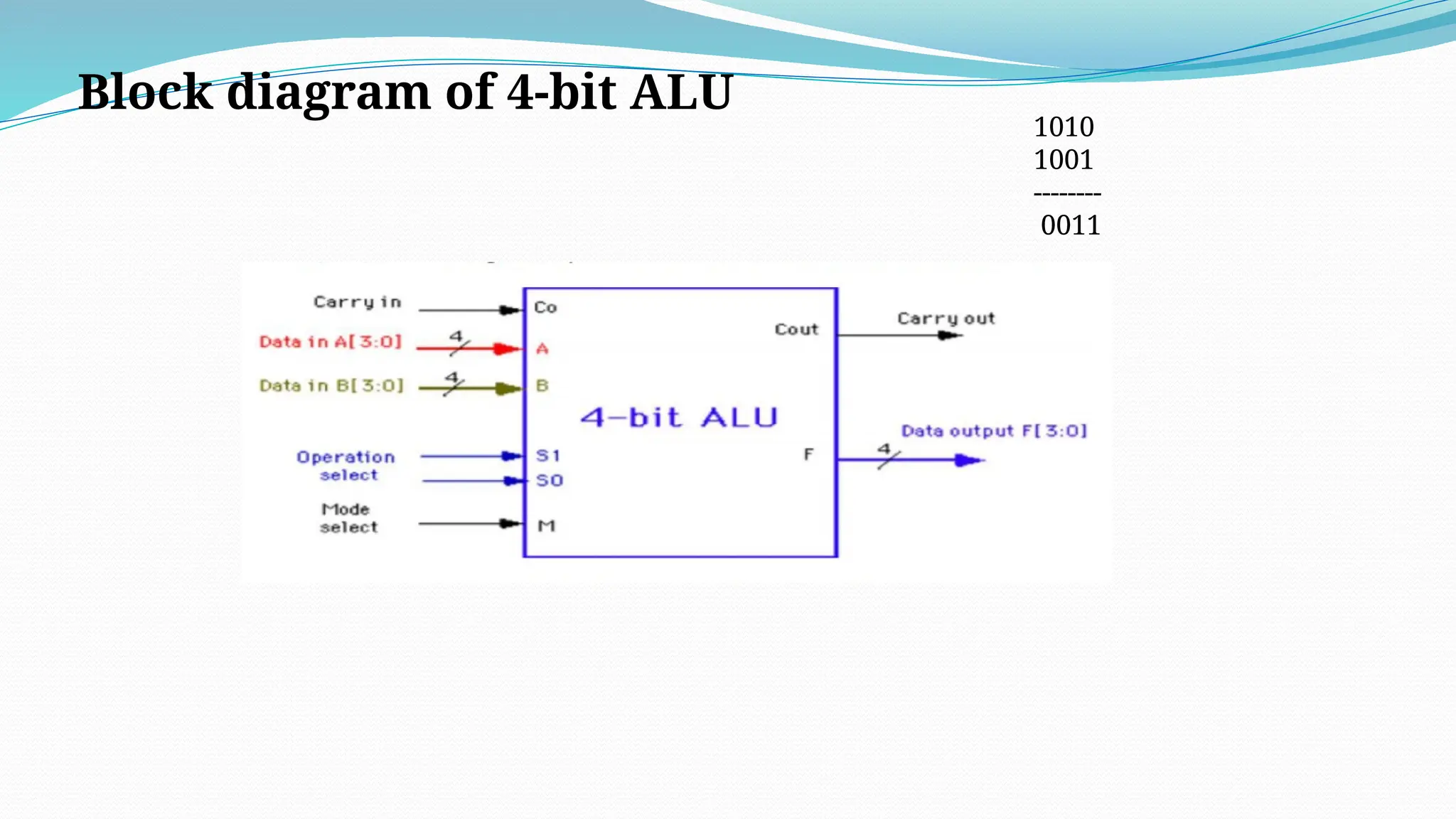
ALU DESIGN
 An Arithmetic and Logic Unit (ALU) is a combinational circuit
that performs logic and arithmetic micro-operations on a pair of
n-bit operands (ex. A[3:0] and B[3:0]). The operations performed
by an ALU are controlled by a set of function select inputs.
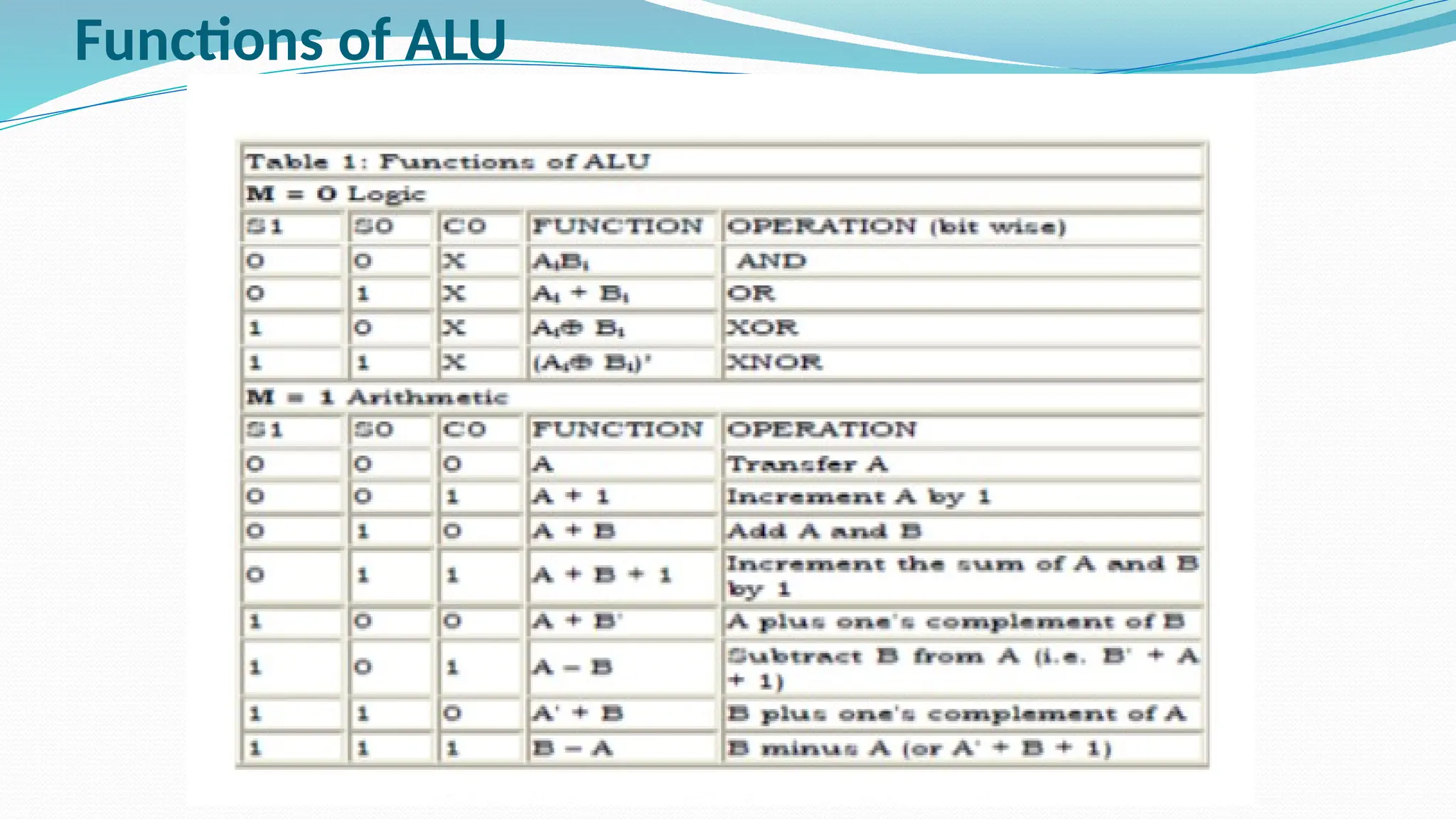
 Design a 4-bit ALU with 3 function-select inputs: Mode M, Select
S1 and S0 inputs. The mode input M selects between a Logic
(M=0) and Arithmetic (M=1) operation. The functions performed
by the ALU are specified in Table I.
Block diagram of 4-bit ALU
1010
1001
--------
0011
Functions of ALU
ADDRESSING MODES
 Programs are normally written in a high-level language, which
enables the programmer to use constants, local and global
variables, pointers, and arrays. When translating a high-level
language program into assembly language, the compiler must be
able to implement these constructs using the facilities provided in
the instruction set of the computer in which the program will be
run. The different ways in which the location of an operand is
specified in an instruction are referred to as addressing modes.
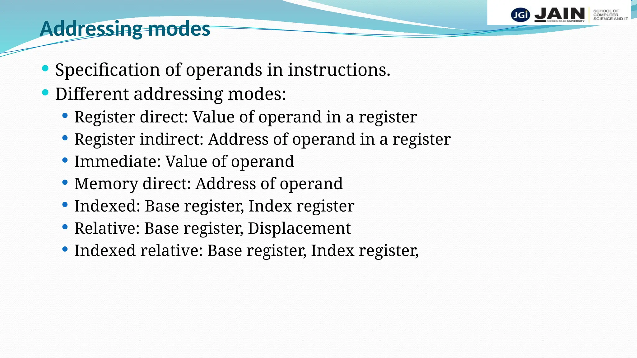
Addressing modes
 Specification of operands in instructions.
 Different addressing modes:
 Register direct: Value of operand in a register
 Register indirect: Address of operand in a register
 Immediate: Value of operand
 Memory direct: Address of operand
 Indexed: Base register, Index register
 Relative: Base register, Displacement
 Indexed relative: Base register, Index register,
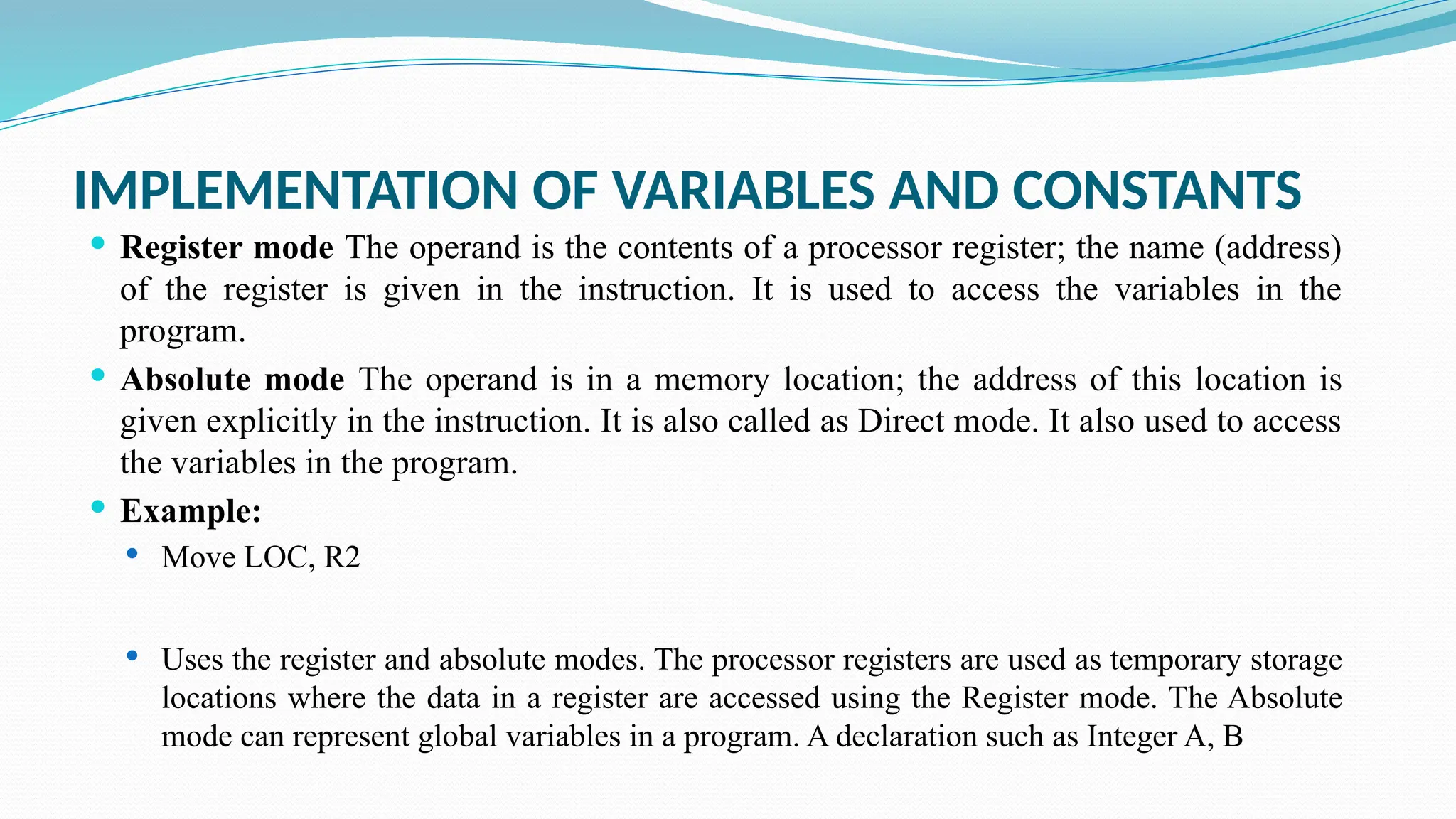
IMPLEMENTATION OF VARIABLES AND CONSTANTS
 Register mode The operand is the contents of a processor register; the name (address)
of the register is given in the instruction. It is used to access the variables in the
program.
 Absolute mode The operand is in a memory location; the address of this location is
given explicitly in the instruction. It is also called as Direct mode. It also used to access
the variables in the program.
 Example:
 Move LOC, R2
 Uses the register and absolute modes. The processor registers are used as temporary storage
locations where the data in a register are accessed using the Register mode. The Absolute
mode can represent global variables in a program. A declaration such as Integer A, B
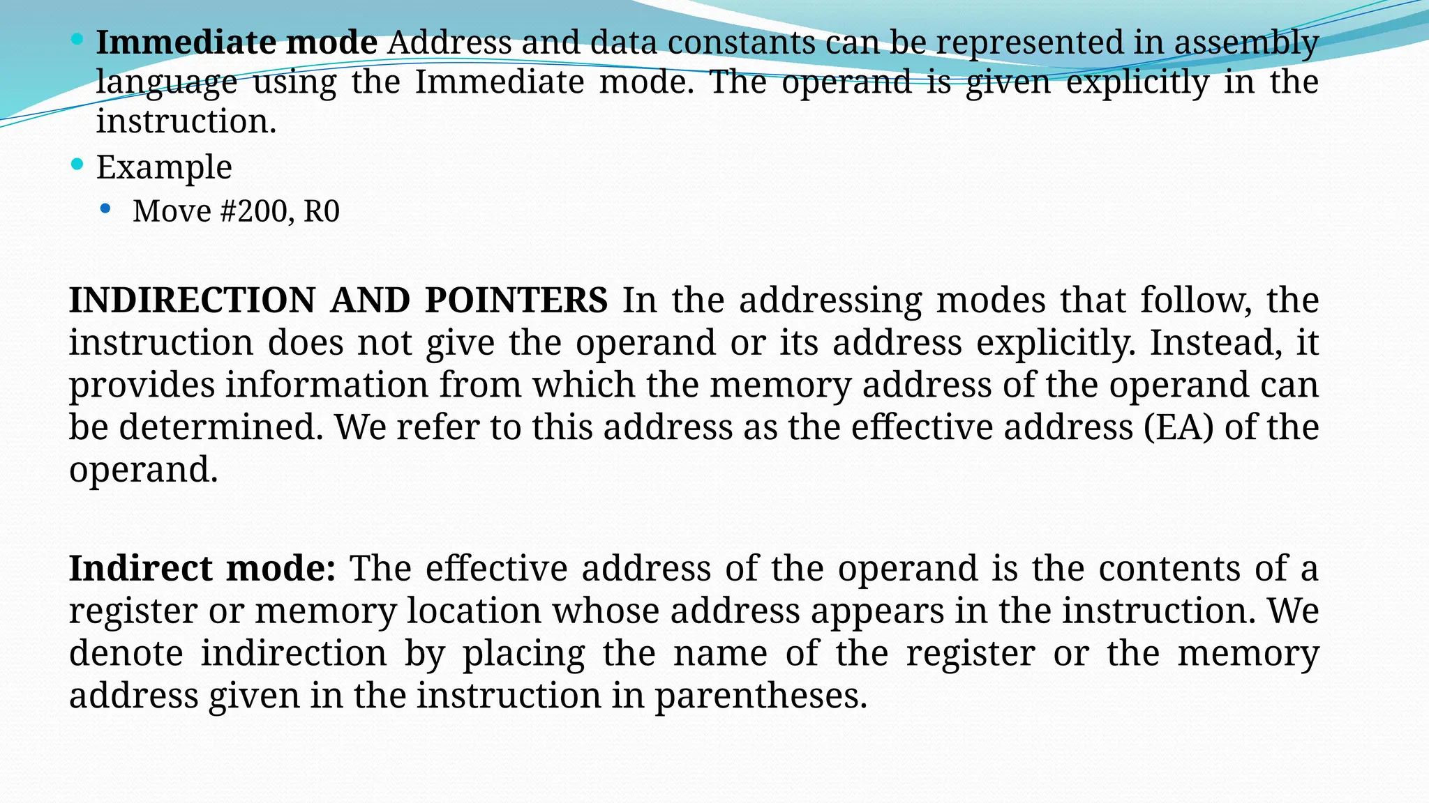
 Immediate mode Address and data constants can be represented in assembly
language using the Immediate mode. The operand is given explicitly in the
instruction.
 Example
 Move #200, R0
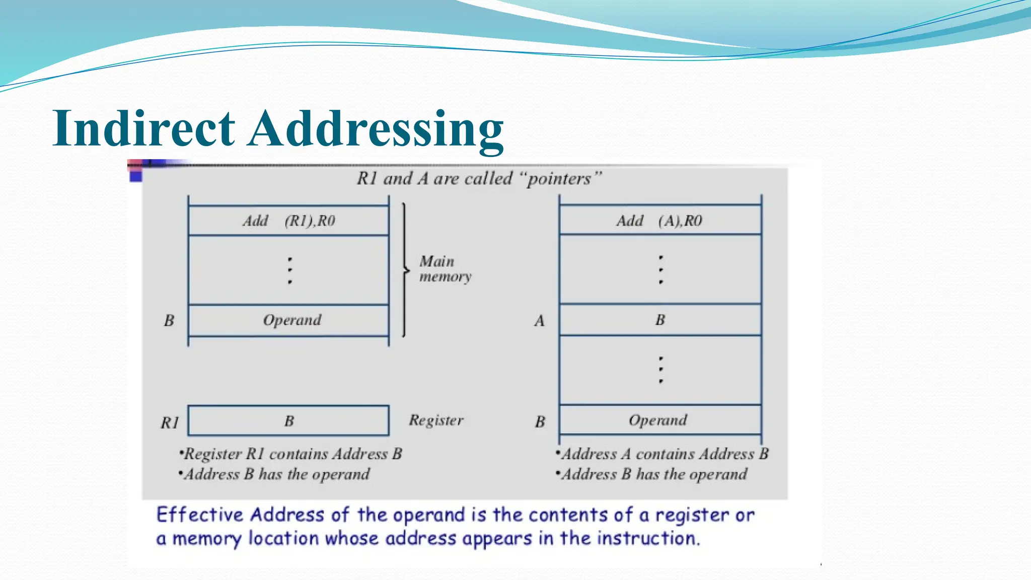
INDIRECTION AND POINTERS In the addressing modes that follow, the
instruction does not give the operand or its address explicitly. Instead, it
provides information from which the memory address of the operand can
be determined. We refer to this address as the effective address (EA) of the
operand.
Indirect mode: The effective address of the operand is the contents of a
register or memory location whose address appears in the instruction. We
denote indirection by placing the name of the register or the memory
address given in the instruction in parentheses.
Indirect Addressing
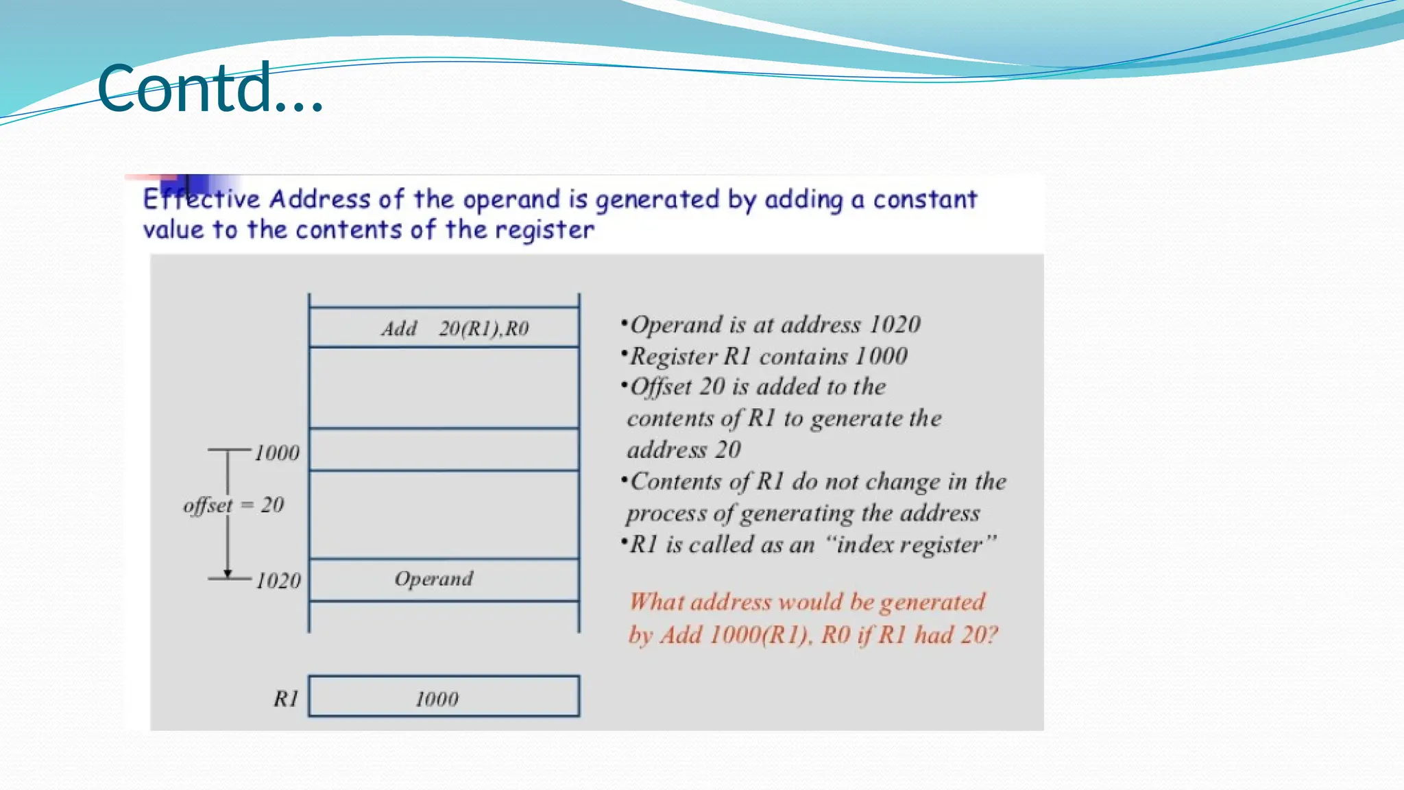
INDEXING AND ARRAYS
 It is useful in dealing with lists and arrays.
Index mode
The effective address of the operand is generated by adding a
constant value to the contents of a register. The register used may
be either a special register provided for this purpose, or, more
commonly; it may be any one of a set of general-purpose registers
in the processor.
In either case, it is referred to as an index register. We indicate the
Index mode symbolically as X (Ri) where X denotes the constant
value contained in the instruction and Ri is the name of the
register involved. The effective address of the operand
is given by
EA = X + [Ri ].
Contd…
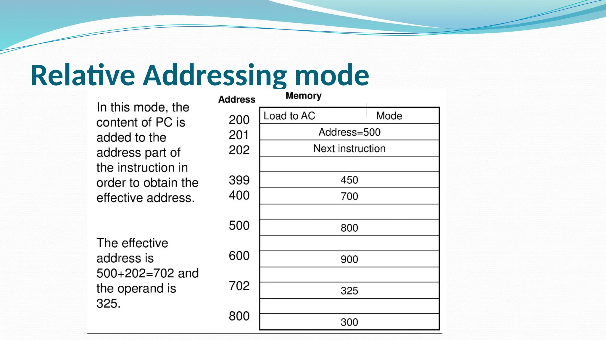
Relative Addressing mode
61
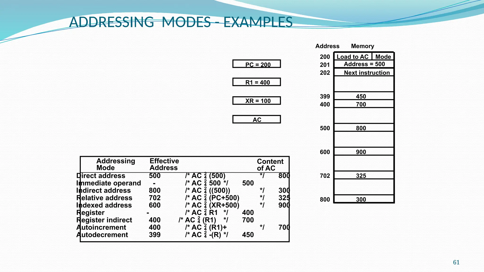
ADDRESSING MODES - EXAMPLES
Addressing
Mode
Effective
Address
Content
of AC
Direct address 500 /* AC  (500) */ 800
Immediate operand - /* AC  500 */ 500
Indirect address 800 /* AC  ((500)) */ 300
Relative address 702 /* AC  (PC+500) */ 325
Indexed address 600 /* AC  (XR+500) */ 900
Register - /* AC  R1 */ 400
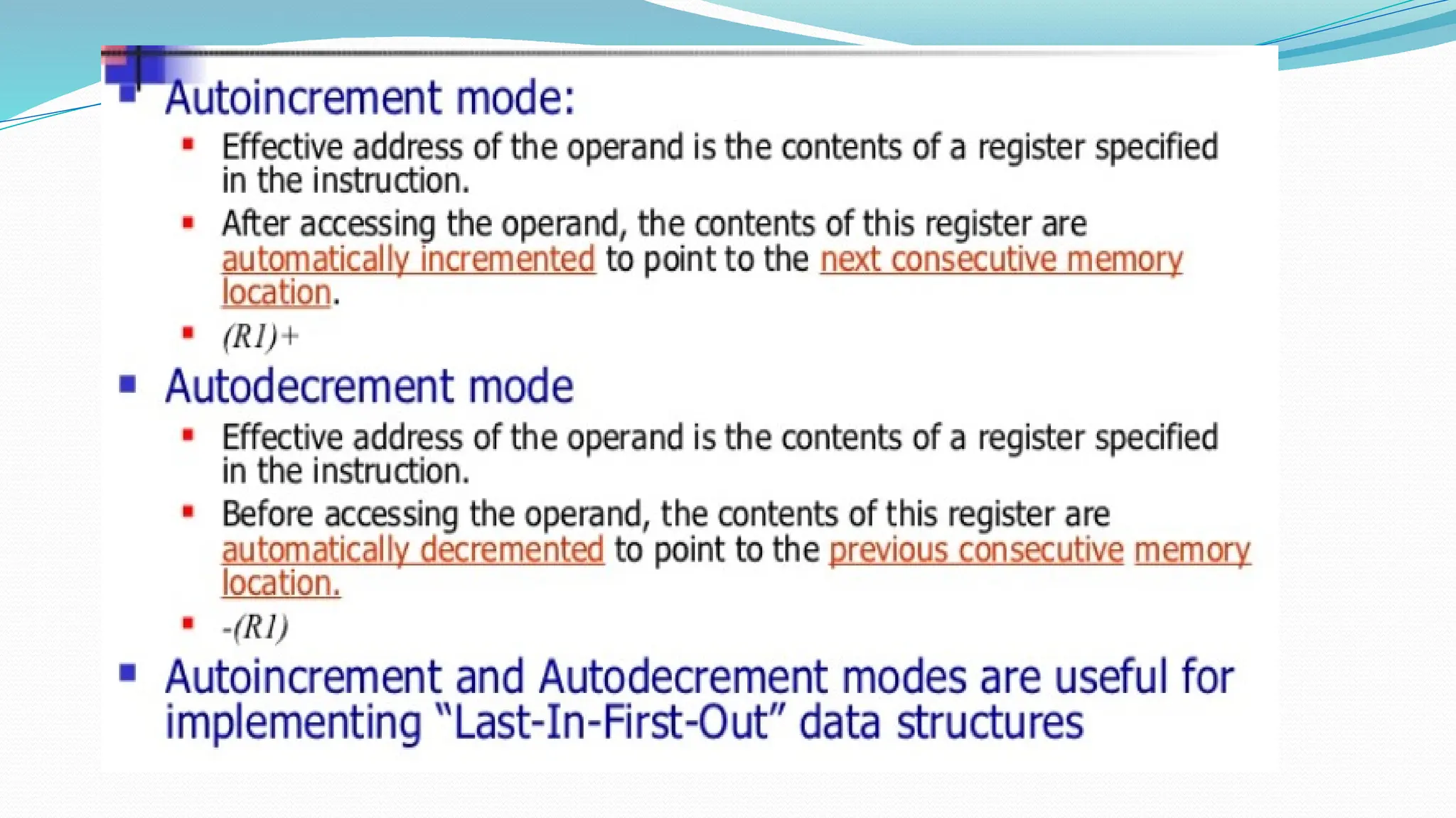
Register indirect 400 /* AC  (R1) */ 700
Autoincrement 400 /* AC  (R1)+ */ 700
Autodecrement 399 /* AC  -(R) */ 450
Load to AC Mode
Address = 500
Next instruction
200
201
202
399
400
450
700
500 800
600 900
702 325
800 300
Memory
Address
PC = 200
R1 = 400
XR = 100
AC
62
DATA TRANSFER INSTRUCTIONS
Load LD
Store ST
Move MOV
Exchange XCH
Input IN
Output OUT
Push PUSH
Pop POP
Name Mnemonic
Typical Data Transfer Instructions
Direct address LD ADR AC M[ADR]
Indirect address LD @ADR AC  M[M[ADR]]
Relative address LD $ADR AC  M[PC + ADR]
Immediate operand LD #NBR AC  NBR
Index addressing LD ADR(X) AC  M[ADR + XR]
Register LD R1 AC  R1
Register indirect LD (R1) AC  M[R1]
Autoincrement LD (R1)+ AC  M[R1], R1  R1 + 1
Autodecrement LD -(R1) R1  R1 - 1, AC  M[R1]
Mode
Assembly
Convention Register Transfer
Data Transfer Instructions with Different Addressing Modes
63
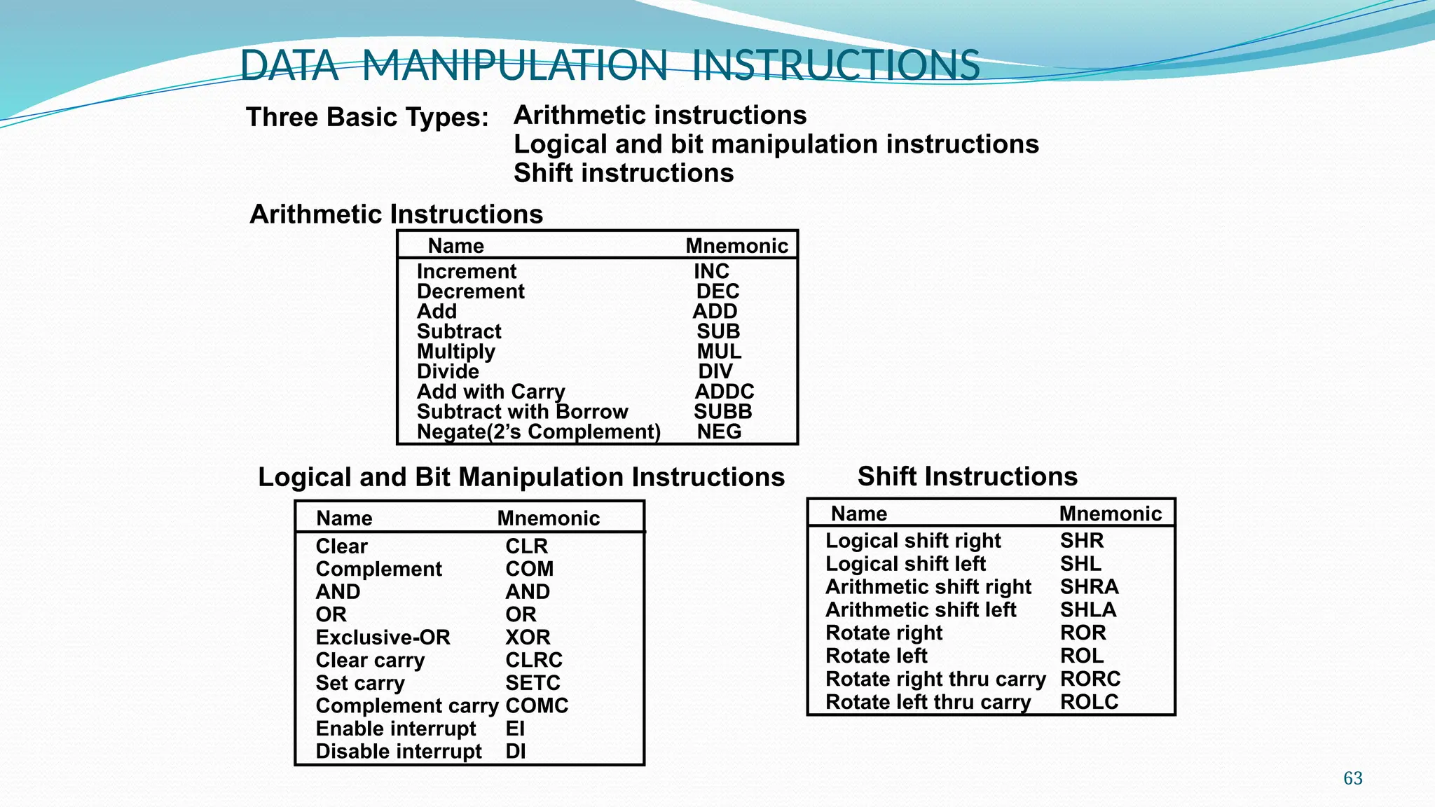
DATA MANIPULATION INSTRUCTIONS
Three Basic Types: Arithmetic instructions
Logical and bit manipulation instructions
Shift instructions
Arithmetic Instructions
Name Mnemonic
Clear CLR
Complement COM
AND AND
OR OR
Exclusive-OR XOR
Clear carry CLRC
Set carry SETC
Complement carry COMC
Enable interrupt EI
Disable interrupt DI
Name Mnemonic
Logical shift right SHR
Logical shift left SHL
Arithmetic shift right SHRA
Arithmetic shift left SHLA
Rotate right ROR
Rotate left ROL
Rotate right thru carry RORC
Rotate left thru carry ROLC
Name Mnemonic
Logical and Bit Manipulation Instructions Shift Instructions
Increment INC
Decrement DEC
Add ADD
Subtract SUB
Multiply MUL
Divide DIV
Add with Carry ADDC
Subtract with Borrow SUBB
Negate(2’s Complement) NEG
Generic Addressing Modes
65
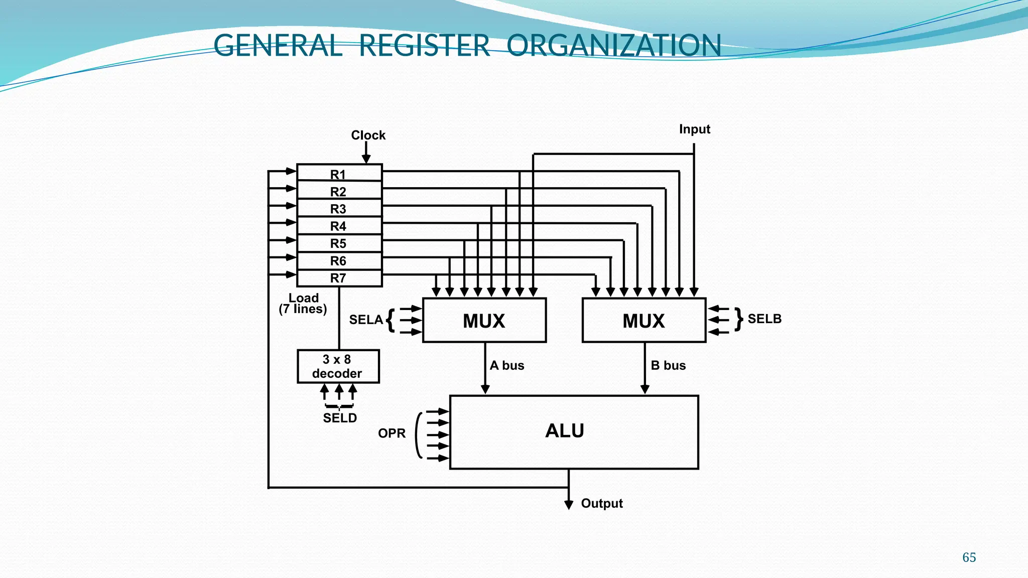
GENERAL REGISTER ORGANIZATION
MUX
SELA{ MUX }SELB
ALU
OPR
R1
R2
R3
R4
R5
R6
R7
Input
3 x 8
decoder
SELD
Load
(7 lines)
Output
A bus B bus
Clock
66
OPERATION OF CONTROL UNIT
The control unit directs the information flow through ALU by:
- Selecting various Components in the system
- Selecting the Function of ALU
Example: R1 <- R2 + R3
[1] MUX A selector (SELA): BUS A  R2
[2] MUX B selector (SELB): BUS B  R3
[3] ALU operation selector (OPR): ALU to ADD
[4] Decoder destination selector (SELD): R1  Out Bus
Control Word
Encoding of register selection fields
Binary
Code SELA SELB SELD
000 Input Input None
001 R1 R1 R1
010 R2 R2 R2
011 R3 R3 R3
100 R4 R4 R4
101 R5 R5 R5
110 R6 R6 R6
111 R7 R7 R7
SELA SELB SELD OPR
3 3 3 5
67
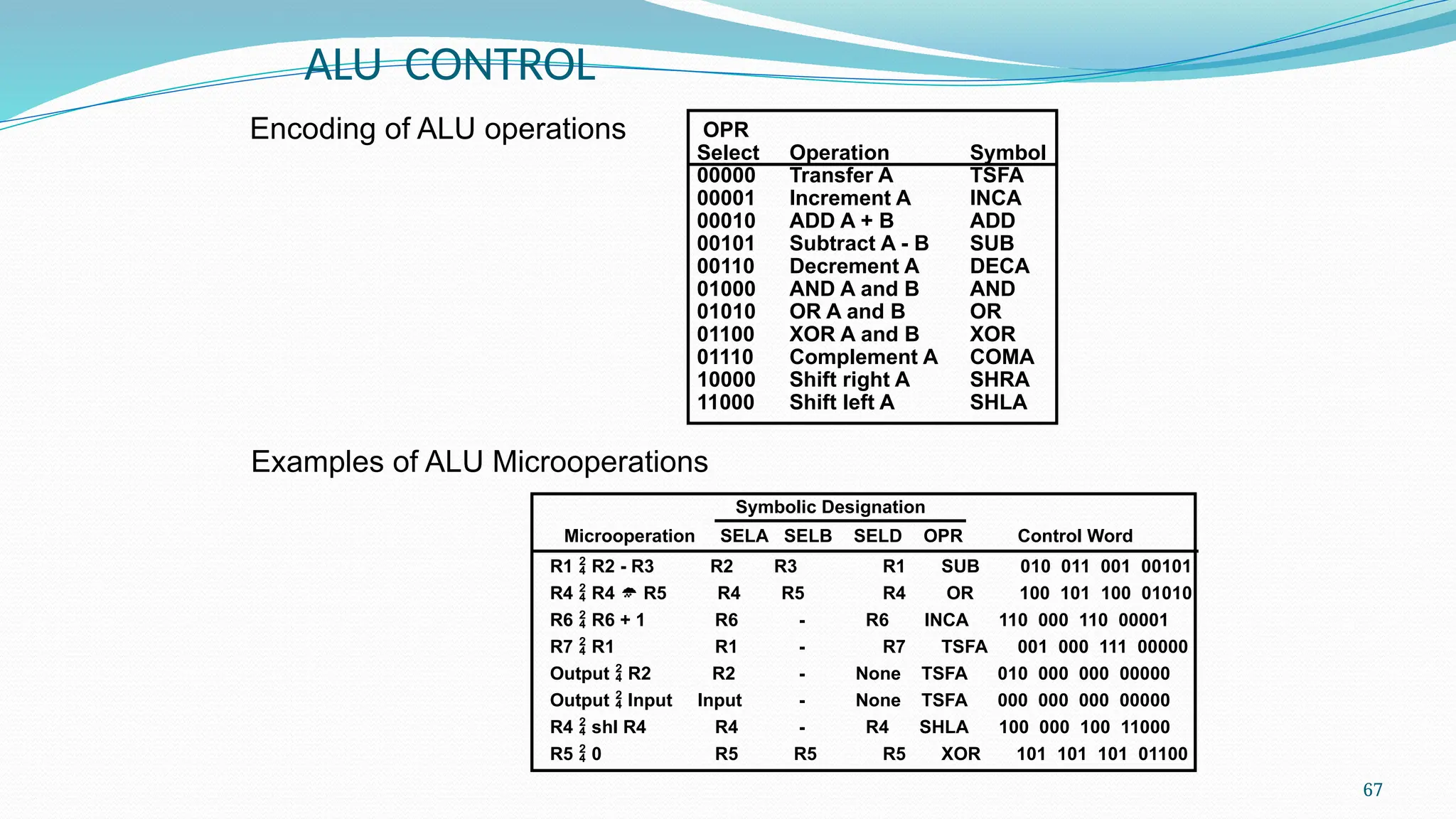
ALU CONTROL
Encoding of ALU operations OPR
Select Operation Symbol
00000 Transfer A TSFA
00001 Increment A INCA
00010 ADD A + B ADD
00101 Subtract A - B SUB
00110 Decrement A DECA
01000 AND A and B AND
01010 OR A and B OR
01100 XOR A and B XOR
01110 Complement A COMA
10000 Shift right A SHRA
11000 Shift left A SHLA
Examples of ALU Microoperations
Symbolic Designation
Microoperation SELA SELB SELD OPR Control Word
R1  R2 - R3 R2 R3 R1 SUB 010 011 001 00101
R4  R4  R5 R4 R5 R4 OR 100 101 100 01010
R6  R6 + 1 R6 - R6 INCA 110 000 110 00001
R7  R1 R1 - R7 TSFA 001 000 111 00000
Output  R2 R2 - None TSFA 010 000 000 00000
Output  Input Input - None TSFA 000 000 000 00000
R4  shl R4 R4 - R4 SHLA 100 000 100 11000
R5  0 R5 R5 R5 XOR 101 101 101 01100
68
REGISTER STACK ORGANIZATION
Register Stack
Push, Pop operations
/* Initially, SP = 0, EMPTY = 1, FULL = 0 */
PUSH POP
SP  SP + 1 DR  M[SP]
M[SP]  DR SP  SP - 1
If (SP = 0) then (FULL  1) If (SP = 0) then (EMPTY  1)
EMPTY  0 FULL  0
Stack
- Very useful feature for nested subroutines, nested loops control
- Also efficient for arithmetic expression evaluation
- Storage which can be accessed in LIFO
- Pointer: SP
- Only PUSH and POP operations are applicable
A
B
C
0
1
2
3
4
63
Address
FULL EMPTY
SP
DR
Flags
Stack pointer
stack
69
MEMORY STACK ORGANIZATION
- A portion of memory is used as a stack with a
processor register as a stack pointer
- PUSH: SP  SP - 1
M[SP]  DR
- POP: DR  M[SP]
SP  SP + 1
- Most computers do not provide hardware to check
stack overflow (full stack) or underflow(empty stack)
Memory with Program, Data,
and Stack Segments
DR
4001
4000
3999
3998
3997
3000
Data
(operands)
Program
(instructions)
1000
PC
AR
SP
stack
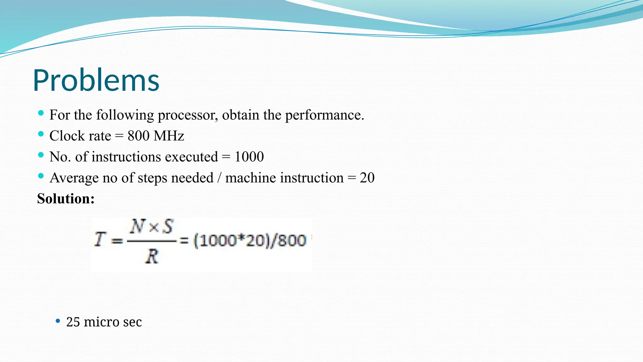
Problems
 For the following processor, obtain the performance.
 Clock rate = 800 MHz
 No. of instructions executed = 1000
 Average no of steps needed / machine instruction = 20
Solution:
 25 micro sec
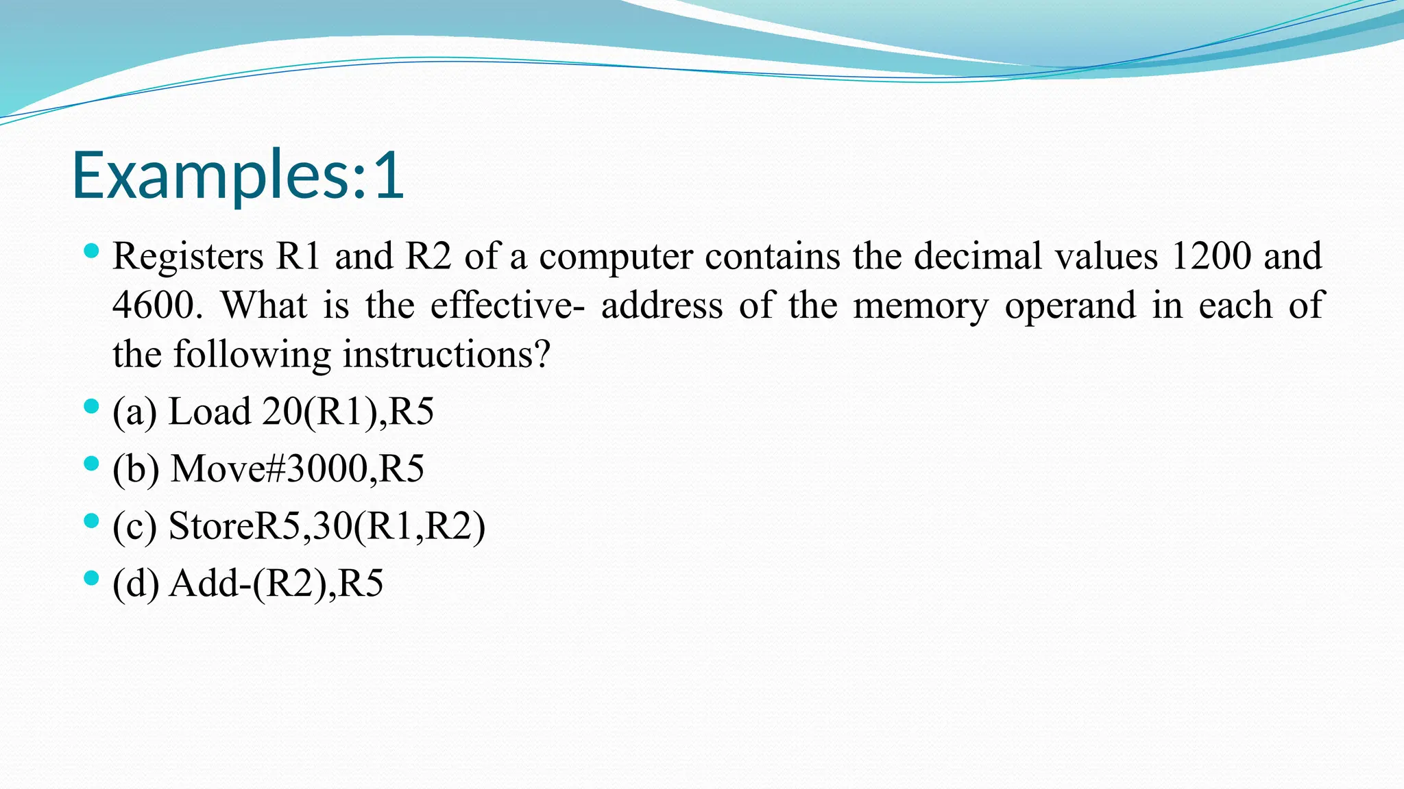
Examples:1
 Registers R1 and R2 of a computer contains the decimal values 1200 and
4600. What is the effective- address of the memory operand in each of
the following instructions?
 (a) Load 20(R1),R5
 (b) Move#3000,R5
 (c) StoreR5,30(R1,R2)
 (d) Add-(R2),R5
Solution
 EA = [R1]+Offset=1200+20 = 1220
 (b) EA = 3000
 (c) EA = [R1]+[R2]+Offset = 1200+4600+30=5830
 (d) EA = [R2]-1 = 4599

module1_CA_for use of tribal network .pptx

  • 1.
  • 2.
    Text & ReferenceBooks T1 M.Moris Mano, (2007), “Computer Systems Architecture”, Pearson/PHI, IIIrd Edition (Module 1,2 & 3) T2 Richard Y. Kain, (2011), “Advanced Computer Architecture a Systems Design Approach”, PHI (Module 4 &5) R1 John L. Hennessy and David A. Patterson, (2012), “Computer Architecture a quantitative approach”, Fifth Edition Elsevier R2 Kai Hwang and Faye Briggs, (2000), “Computer Architecture and Parallel Processing”, Mc Graw- Hill International Edition R3 Carl Hamacher, Zvonko Vranesic, Safwat Zaky, (2002), “Computer Organization”, McGraw Hill, Vth Edition R4 Andrew S. Tanenbaum, (2006), “Structured Computer Organization” PHI/Pearson, 4th Edition R5 Safwat Zaky and Naraig Manjikian, (2012), “Computer Organization and Embedded Systems”, Tata McGraw Hill, Sixth Edition
  • 3.
    Introduction  A computercan be defined as a fast electronic calculating machine that accepts the (data) digitized input information process it as per the list of internally stored instructions and produces the resulting information. List of instructions are called programs & internal storage is called computer memory.
  • 4.
    Computer Architecture  ComputerArchitecture is a set of rules and methods that describe the functionality, organization, and implementation of computer systems.  Some definitions of architecture define it as describing the capabilities and programming model of a computer but not a particular implementation.  In other definitions computer architecture involves instruction set architecture design, micro architecture design, implementation. logic design, and implementation
  • 5.
    Types of computer: Personal computers: - This is the most common type found in homes, schools, Business offices etc., It is the most common type of desk top computers with processing and storage units along with various input and output devices.  Note book computers: - These are compact and portable versions of PC.  Work stations: - These have high resolution input/output (I/O) graphics capability, but with same dimensions as that of desktop computer. These are used in engineering applications of interactive design work.  Enterprise systems: - These are used for business data processing in medium to large corporations that require much more computing power and storage capacity than work stations. Internet associated with servers have become a dominant worldwide source of all types of information.  Super computers: - These are used for large scale numerical calculations required in the applications like weather forecasting etc.,
  • 6.
    Functional unit  Acomputer consists of five functionally independent main parts input, memory, arithmetic logic unit (ALU), output and control unit. Fig. Functional units of computer
  • 7.
     Input deviceaccepts the coded information as source program i.e. high level language.  This is either stored in the memory or immediately used by the processor to perform the desired operations.  The program stored in the memory determines the processing steps. Basically the computer converts one source program to an object program. i.e. into machine language.  Finally the results are sent to the outside world through output device.  All of these actions are coordinated by the control unit.
  • 8.
    Input Unit  Thesource program/high level language program/coded information/simply data is fed to a computer through input devices keyboard is a most common type.  Whenever a key is pressed, one corresponding word or number is translated into its equivalent binary code over a cable & fed either to memory or processor. E.g. Joysticks, trackballs, mouse, scanners etc are other input devices.
  • 10.
    Memory unit  Itsfunction into store programs and data. It is basically to two types 1. Primary memory 2. Secondary memory Primary memory:  It is the one exclusively associated with the processor and operates at the electronics speeds programs must be stored in this memory while they are being executed.  The memory contains a large number of semiconductors storage cells. Each capable of storing one bit of information. These are processed in a group of fixed site called word.
  • 11.
     To provideeasy access to a word in memory, a distinct address is associated with each word location.  Addresses are numbers that identify memory location. Number of bits in each word is called word length of the computer. Programs must reside in the memory during execution.  Instructions and data can be written into the memory or read out under the control of processor.  Memory in which any location can be reached in a short and fixed amount of time after specifying its address is called random-access memory (RAM).  The time required to access one word in called memory access time. Memory which is only readable by the user and contents of which can’t be altered is called read only memory (ROM) it contains operating system.
  • 12.
    Secondary memory  Itis used where large amounts of data & programs must be stored, particularly information that is accessed infrequently.  Examples: Magnetic disks & tapes, optical disks (ie CD-ROM’s), floppies etc.,
  • 14.
    Arithmetic logic unit(ALU)  Most of the computer operators are executed in ALU of the processor like addition, subtraction, division, multiplication, etc. the operands are brought into the ALU from memory and stored in high-speed storage elements called register.  Then according to the instructions, the operation is performed in the required sequence. The control and the ALU are may times faster than other devices connected to a computer system.  This enables a single processor to control a number of external devices such as keyboards, displays, magnetic and optical disks, sensors and other mechanical controllers.
  • 15.
    Output unit  Theseactually are the counterparts of input unit. Its basic function is to send the processed results to the outside world.  Examples:- Printer, speakers, monitor etc.
  • 16.
    Control unit  Iteffectively is the nerve center that sends signals to other units and senses their states.  The actual timing signals that govern the transfer of data between input unit, processor, memory and output unit are generated by the control unit.
  • 17.
    17 Hardware – SoftwareInterface Application software Systems software Operating system compiler assembler User Programs user writes and runs Hardwar e
  • 19.
    19 Instruction Set Architecture(ISA)  A set of assembly language instructions (ISA) provides a link between software and hardware.Ex. C=a+b  Given an instruction set, software programmers and hardware engineers work more or less independently.  ISA is designed to extract the most performance out of the available hardware technology. Defines data transfer modes between registers, memory and I/O Types of ISA: RISC, CISC, VLIW, Superscalar Examples:  IBM370/X86/Pentium/K6 (CISC), PowerPC (Superscalar)  Alpha (Superscalar), MIPS (RISC and Superscalar)  Sparc (RISC), UltraSparc (Superscalar)
  • 20.
    20 RISC: REDUCED INSTRUCTIONSET COMPUTERS Historical Background IBM System/360, 1964 - The real beginning of modern computer architecture - Distinction between Architecture and Implementation - Architecture: The abstract structure of a computer seen by an assembly-language programmer High-Level Language Instruction Set Hardware Compiler -program Architecture Implementation Continuing growth in semiconductor memory and microprogramming -> A much richer and complicated instruction sets => CISC(Complex Instruction Set Computer) - Arguments advanced at that time Richer instruction sets would simplify compilers Richer instruction sets would alleviate the software crisis - move as much functions to the hardware as possible - close Semantic Gap between machine language and the high-level language Richer instruction sets would improve the architecture quality
  • 21.
    What is CISC? •CISC is an acronym for Complex Instruction Set Computer and are chips that are easy to program and which make efficient use of memory. Since the earliest machines were programmed in assembly language and memory was slow and expensive, the CISC philosophy made sense • Most common microprocessor designs such as the Intel 80x86 and Motorola 68K series followed the CISC philosophy. • But recent changes in software and hardware technology have forced a re- examination of CISC and many modern CISC processors are hybrids, implementing many RISC principles. • CISC was developed to make compiler development simpler. It shifts most of the burden of generating machine instructions to the processor. For example, instead of having to make a compiler write long machine instructions to calculate a square-root, a CISC processor would have a built-in ability to do this.
  • 22.
    22 COMPLEX INSTRUCTION SETCOMPUTERS: CISC High Performance General Purpose Instructions Characteristics of CISC: 1. A large number of instructions (from 100-250 usually) 2. Some instructions that performs a certain tasks are not used frequently. 3. Many addressing modes are used (5 to 20) 4. Variable length instruction format. 5. Instructions that manipulate operands in memory. 1. C=a+b 2. Ex: ADD A B
  • 23.
    23 CHARACTERISTICS OF RISC RISCCharacteristics - Relatively few instructions - Relatively few addressing modes - Memory access limited to load and store instructions - All operations done within the registers of the CPU - Fixed-length, easily decoded instruction format - Single-cycle instruction format - Hardwired rather than microprogrammed control - A relatively large numbers of registers in the processor unit. - Efficient instruction pipeline - Compiler support: provides efficient translation of high-level language programs into machine language programs. More RISC Characteristics Advantages of RISC - VLSI Realization - Computing Speed - Design Costs and Reliability - High Level Language Support
  • 24.
    24 Contd. The main characteristicsof CISC microprocessors are: • Extensive instructions. • Complex and efficient machine instructions. • Micro encoding of the machine instructions. • Extensive addressing capabilities for memory operations. • Relatively few registers. In comparison, RISC processors are more or less the opposite of the above: • Reduced instruction set. • Less complex, simple instructions. • Hardwired control unit and machine instructions. • Few addressing schemes for memory operands with only two basic instructions, LOAD and STORE
  • 25.
    CISC versus RISC CISCRISC Emphasis on hardware Emphasis on software Includes multi-clock complex instructions Single-clock, reduced instruction only Memory-to-memory: "LOAD" and "STORE" incorporated in instructions Register to register: "LOAD" and "STORE" are independent instructions Small code sizes, high cycles per second Low cycles per second, large code sizes Transistors used for storing complex instructions Spends more transistors on memory registers
  • 27.
     The mostimportant measure of a computer is how quickly it can execute programs.  Three factors affect performance:  Hardware design  Instruction set  Compiler Performance 27
  • 28.
    Processor time toexecute a program depends on the hardware involved in the execution of individual machine instructions. Main memory Processor Bus Cache memory The processor cache. Performance 28
  • 29.
     The processorand a relatively small cache memory can be fabricated on a single integrated circuit chip.  Speed  Cost  Memory management Performance 29
  • 30.
    Processor Clock 30  Clock, clockcycle, and clock rate  The execution of each instruction is divided into several steps, each of which completes in one clock cycle.  Hertz – cycles per second
  • 31.
    Basic Performance Equation 31 T – processor time required to execute a program that has been prepared in high-level language N – number of actual machine language instructions needed to complete the execution (note: loop) S – average number of basic steps needed to execute one machine instruction. Each step completes in one clock cycle R – clock rate Note: these are not independent to each other T  N  S     R
  • 32.
    Clock Rate 32  Increaseclock rate   Improve the integrated-circuit (IC) technology to make the circuits faster Reduce the amount of processing done in one basic step (however, this may increase the number of basic steps needed)  Increases in R that are entirely caused by improvements in IC technology affect all aspects of the processor’s operation equally except the time to access the main memory.
  • 33.
    Compiler 33  A compilertranslates a high-level language program into a sequence of machine instructions. To reduce N, we need a suitable machine instruction set and a compiler that makes good use of it. Goal – reduce N×S A compiler may not be designed for a specific processor; however, a high-quality compiler is usually designed for, and with, a specific processor.   
  • 34.
    Performance Measurement 34    T isdifficult to compute. Measure computer performance using benchmark programs. System Performance Evaluation Corporation (SPEC) selects and publishes representative application programs for different application domains, together with test results for many commercially available computers. Compile and run (no simulation) Reference computer   S P E C rating  Running time on the reference computer Running time on the computer under test n 1 SPEC rating  ( SPECi ) n i1
  • 35.
    Amdahl's Law Amdahl's lawstates that performance improvement to be gained by using a faster mode of execution is limited by the fraction of time the faster mode can be used. Using this law, the performance gain that can be obtained by improving some portion of the computer can be calculated using the following formula. Performance of entire task using the enhancement when possible Speedup = --------------------------------------------------------- Performance for the entire task without using the enhancement
  • 36.
    BUS STRUCTURES  Busis a group of lines that serves as a connection path for several individual parts of a computer to transfer the data between them. To achieve a reasonable speed of the operation, a computer must be organized so that, All its units can handle one full word of data at a given time. Single Bus Structure Multiple Bus structure System using multiple buses results in concurrency as it allows two or more transfer at the same time. This leads to high performance but at increased cost.
  • 37.
    INSTRUCTION AND INSTRUCTIONSEQUENCING  A computer must have instruction capable of performing four types of basic operations such as Data transfer between the memory and the processor registers.  Arithmetic and logic operation on data Program sequencing and control I/O transfers To understand the first two types of instruction, we need to know some notations.  Register Transfer Notation  Assembly Language Notation
  • 38.
    Register Transfer Notation(RTN)  Data transfer can be represented by standard notations given below.  Processor registers are represented by notations R0, R1, R2.  Address of the memory locations are represented by names such as LOC, PLACE, MEM etc..  I/O registers are represented by names such as DATAIN, DATAOUT.  The content of memory locations are denoted by placing square bracket around the name of the register.  Example 1: R1 [LOC] ←  This expression states that the contents of memory location LOC are transferred into the processor register R1.  Example 2: R3 [R1] + [R2] ←  This expression states that the contents of processor registers R1 and R2 are added and the result is stored into the processor register R3. This type of notation is known as Register Transfer Notation (RTN).
  • 39.
    Assembly Language Notation To represent machine instructions, assembly language uses statements as shown below To transfer the data from memory location LOC to processor register R1  Move LOC, R1 ( Syntax: MOVE LOCATION, REGISTER)  To add two numbers in register R1 and R2 and to place their sum in register R3  ADD R1, R2, R3 (: R3 [R1] + [R2] ← )
  • 40.
    General Purpose Registers •Instructions register (IR) • Program counter (PC) • Memory address registers (MAR) • Memory data register (MDR)
  • 41.
     Instruction registers(IR): IR holds the instruction that is currently being executed by the processor. Its output is available to the control circuits, which generates the timing signals that controls various processing elements involved in executing the instruction.  Program counter (PC): It is a special purpose register that contains the address of the next instruction to be fetched and executed. During the execution of one instruction PC is updated to point the address of the next instruction to be fetched and executed. It keeps track of the execution of a program.  Memory address registers (MAR): The MAR holds the address of the memory location to be accessed.  Memory data register (MDR): The MDR contains the data to be written into or read from the memory location that is being pointed by MAR. These two registers MAR and MDR facilitates communication between memory and the processor.
  • 42.
    Buffer registers  Bufferregister is an electronic register that is included with the devices to hold the information during transfer. When the processor sends a set of characters to a printer, those contents is transferred to the printer buffer (buffer register for a printer). Once printer buffer is loaded processor and the bus is no longer needed and the processor can be released for other activity.  Purpose of Buffer Register: ✓ Buffer register prevent a high speed processor from being locked to a slow I/O devices. ✓ Buffer register is used which smooth out timing differences among slow and the fast devices. ✓ It allows the processor to switch rapidly from one device to another.
  • 43.
    ISA  Interface betweenthe high level language and the machine language It has the following parts:  Instruction set Addressing modes  Instruction formats  Instruction representation
  • 44.
    Instructions Logical instructions  AND,OR, XOR, Shift Arithmetic instructions Data types Integers: Unsigned, Signed, Byte, Short, Long Real numbers: Single precision (float), Double precision (double) Operations Addition, Subtraction, Multiplication, Division Data transfer instructions Register transfer: Move Memory transfer: Load, Store I/O transfer: In, Out Control transfer instructions • Unconditional branch • Conditional branch • Procedure call • Return
  • 45.
    45 INSTRUCTION FORMAT OP-code field- specifies the operation to be performed Address field - designates memory address(s) or a processor register(s) Mode field - specifies the way the operand or the effective address is determined The number of address fields in the instruction format depends on the internal organization of CPU - The three most common CPU organizations: Single accumulator organization: ADD X /* AC  AC + M[X] */ General register organization: ADD R1, R2, R3 /* R1  R2 + R3 */ ADD R1, R2 /* R1  R1 + R2 */ MOV R1, R2 /* R1  R2 */ ADD R1, X /* R1  R1 + M[X] */ Stack organization: PUSH X /* TOS  M[X] */ ADD Instruction Fields
  • 46.
    46 THREE, and TWO-ADDRESS INSTRUCTIONS Three-AddressInstructions: Program to evaluate X = (A + B) * (C + D) : ADD R1, A, B /* R1  M[A] + M[B] */ ADD R2, C, D /* R2  M[C] + M[D] */ MUL X, R1, R2 /* M[X]  R1 * R2 */ - Results in short programs - Instruction becomes long (many bits) Two-Address Instructions: Program to evaluate X = (A + B) * (C + D) : MOV R1, A /* R1  M[A] */ ADD R1, B /* R1  R1 + M[B] */ MOV R2, C /* R2  M[C] */ ADD R2, D /* R2  R2 + M[D] */ MUL R1, R2 /* R1  R1 * R2 */ MOV X, R1 /* M[X]  R1 */
  • 47.
    47 ONE, and ZERO-ADDRESSINSTRUCTIONS One-Address Instructions: - Use an implied AC register for all data manipulation - Program to evaluate X = (A + B) * (C + D) : LOAD A /* AC  M[A] */ ADD B /* AC  AC + M[B] */ STORE T /* M[T]  AC */ LOAD C /* AC  M[C] */ ADD D /* AC  AC + M[D] */ MUL T /* AC  AC * M[T]*/ STORE X /* M[X]  AC */ Zero-Address Instructions: - Can be found in a stack-organized computer - Program to evaluate X = (A + B) * (C + D) : PUSH A /* TOS  A */ PUSH B /* TOS  B */ ADD /* TOS  (A + B) */ PUSH C /* TOS  C */ PUSH D /* TOS  D */ ADD /* TOS  (C + D) */ MUL /* TOS  (C + D) * (A + B) */ POP X /* M[X]  TOS */
  • 48.
     Complex InstructionSet Computer (CISC) processors: 2 operand instructions and 1 operand instructions Any instruction can use memory operands, Many addressing modes, Complex instruction formats: Varying length instructions , Micro programmed control unit. Reduced Instruction Set Computer (RISC) processors: 3 operand instructions, 2 operand instructions, and 1 operand instructions. Architecture processors: • Only memory transfer instructions (Load and Store) can use memory operands. • All other instructions can use register operands only. – A few addressing modes. – Simple instruction formats: Fixed length instructions. – Hardwired control unit.
  • 49.
    ALU DESIGN  AnArithmetic and Logic Unit (ALU) is a combinational circuit that performs logic and arithmetic micro-operations on a pair of n-bit operands (ex. A[3:0] and B[3:0]). The operations performed by an ALU are controlled by a set of function select inputs.  Design a 4-bit ALU with 3 function-select inputs: Mode M, Select S1 and S0 inputs. The mode input M selects between a Logic (M=0) and Arithmetic (M=1) operation. The functions performed by the ALU are specified in Table I.
  • 50.
    Block diagram of4-bit ALU 1010 1001 -------- 0011
  • 51.
  • 52.
    ADDRESSING MODES  Programsare normally written in a high-level language, which enables the programmer to use constants, local and global variables, pointers, and arrays. When translating a high-level language program into assembly language, the compiler must be able to implement these constructs using the facilities provided in the instruction set of the computer in which the program will be run. The different ways in which the location of an operand is specified in an instruction are referred to as addressing modes.
  • 53.
    Addressing modes  Specificationof operands in instructions.  Different addressing modes:  Register direct: Value of operand in a register  Register indirect: Address of operand in a register  Immediate: Value of operand  Memory direct: Address of operand  Indexed: Base register, Index register  Relative: Base register, Displacement  Indexed relative: Base register, Index register,
  • 54.
    IMPLEMENTATION OF VARIABLESAND CONSTANTS  Register mode The operand is the contents of a processor register; the name (address) of the register is given in the instruction. It is used to access the variables in the program.  Absolute mode The operand is in a memory location; the address of this location is given explicitly in the instruction. It is also called as Direct mode. It also used to access the variables in the program.  Example:  Move LOC, R2  Uses the register and absolute modes. The processor registers are used as temporary storage locations where the data in a register are accessed using the Register mode. The Absolute mode can represent global variables in a program. A declaration such as Integer A, B
  • 55.
     Immediate modeAddress and data constants can be represented in assembly language using the Immediate mode. The operand is given explicitly in the instruction.  Example  Move #200, R0 INDIRECTION AND POINTERS In the addressing modes that follow, the instruction does not give the operand or its address explicitly. Instead, it provides information from which the memory address of the operand can be determined. We refer to this address as the effective address (EA) of the operand. Indirect mode: The effective address of the operand is the contents of a register or memory location whose address appears in the instruction. We denote indirection by placing the name of the register or the memory address given in the instruction in parentheses.
  • 56.
  • 57.
    INDEXING AND ARRAYS It is useful in dealing with lists and arrays. Index mode The effective address of the operand is generated by adding a constant value to the contents of a register. The register used may be either a special register provided for this purpose, or, more commonly; it may be any one of a set of general-purpose registers in the processor. In either case, it is referred to as an index register. We indicate the Index mode symbolically as X (Ri) where X denotes the constant value contained in the instruction and Ri is the name of the register involved. The effective address of the operand is given by EA = X + [Ri ].
  • 58.
  • 59.
  • 61.
    61 ADDRESSING MODES -EXAMPLES Addressing Mode Effective Address Content of AC Direct address 500 /* AC  (500) */ 800 Immediate operand - /* AC  500 */ 500 Indirect address 800 /* AC  ((500)) */ 300 Relative address 702 /* AC  (PC+500) */ 325 Indexed address 600 /* AC  (XR+500) */ 900 Register - /* AC  R1 */ 400 Register indirect 400 /* AC  (R1) */ 700 Autoincrement 400 /* AC  (R1)+ */ 700 Autodecrement 399 /* AC  -(R) */ 450 Load to AC Mode Address = 500 Next instruction 200 201 202 399 400 450 700 500 800 600 900 702 325 800 300 Memory Address PC = 200 R1 = 400 XR = 100 AC
  • 62.
    62 DATA TRANSFER INSTRUCTIONS LoadLD Store ST Move MOV Exchange XCH Input IN Output OUT Push PUSH Pop POP Name Mnemonic Typical Data Transfer Instructions Direct address LD ADR AC M[ADR] Indirect address LD @ADR AC  M[M[ADR]] Relative address LD $ADR AC  M[PC + ADR] Immediate operand LD #NBR AC  NBR Index addressing LD ADR(X) AC  M[ADR + XR] Register LD R1 AC  R1 Register indirect LD (R1) AC  M[R1] Autoincrement LD (R1)+ AC  M[R1], R1  R1 + 1 Autodecrement LD -(R1) R1  R1 - 1, AC  M[R1] Mode Assembly Convention Register Transfer Data Transfer Instructions with Different Addressing Modes
  • 63.
    63 DATA MANIPULATION INSTRUCTIONS ThreeBasic Types: Arithmetic instructions Logical and bit manipulation instructions Shift instructions Arithmetic Instructions Name Mnemonic Clear CLR Complement COM AND AND OR OR Exclusive-OR XOR Clear carry CLRC Set carry SETC Complement carry COMC Enable interrupt EI Disable interrupt DI Name Mnemonic Logical shift right SHR Logical shift left SHL Arithmetic shift right SHRA Arithmetic shift left SHLA Rotate right ROR Rotate left ROL Rotate right thru carry RORC Rotate left thru carry ROLC Name Mnemonic Logical and Bit Manipulation Instructions Shift Instructions Increment INC Decrement DEC Add ADD Subtract SUB Multiply MUL Divide DIV Add with Carry ADDC Subtract with Borrow SUBB Negate(2’s Complement) NEG
  • 64.
  • 65.
    65 GENERAL REGISTER ORGANIZATION MUX SELA{MUX }SELB ALU OPR R1 R2 R3 R4 R5 R6 R7 Input 3 x 8 decoder SELD Load (7 lines) Output A bus B bus Clock
  • 66.
    66 OPERATION OF CONTROLUNIT The control unit directs the information flow through ALU by: - Selecting various Components in the system - Selecting the Function of ALU Example: R1 <- R2 + R3 [1] MUX A selector (SELA): BUS A  R2 [2] MUX B selector (SELB): BUS B  R3 [3] ALU operation selector (OPR): ALU to ADD [4] Decoder destination selector (SELD): R1  Out Bus Control Word Encoding of register selection fields Binary Code SELA SELB SELD 000 Input Input None 001 R1 R1 R1 010 R2 R2 R2 011 R3 R3 R3 100 R4 R4 R4 101 R5 R5 R5 110 R6 R6 R6 111 R7 R7 R7 SELA SELB SELD OPR 3 3 3 5
  • 67.
    67 ALU CONTROL Encoding ofALU operations OPR Select Operation Symbol 00000 Transfer A TSFA 00001 Increment A INCA 00010 ADD A + B ADD 00101 Subtract A - B SUB 00110 Decrement A DECA 01000 AND A and B AND 01010 OR A and B OR 01100 XOR A and B XOR 01110 Complement A COMA 10000 Shift right A SHRA 11000 Shift left A SHLA Examples of ALU Microoperations Symbolic Designation Microoperation SELA SELB SELD OPR Control Word R1  R2 - R3 R2 R3 R1 SUB 010 011 001 00101 R4  R4  R5 R4 R5 R4 OR 100 101 100 01010 R6  R6 + 1 R6 - R6 INCA 110 000 110 00001 R7  R1 R1 - R7 TSFA 001 000 111 00000 Output  R2 R2 - None TSFA 010 000 000 00000 Output  Input Input - None TSFA 000 000 000 00000 R4  shl R4 R4 - R4 SHLA 100 000 100 11000 R5  0 R5 R5 R5 XOR 101 101 101 01100
  • 68.
    68 REGISTER STACK ORGANIZATION RegisterStack Push, Pop operations /* Initially, SP = 0, EMPTY = 1, FULL = 0 */ PUSH POP SP  SP + 1 DR  M[SP] M[SP]  DR SP  SP - 1 If (SP = 0) then (FULL  1) If (SP = 0) then (EMPTY  1) EMPTY  0 FULL  0 Stack - Very useful feature for nested subroutines, nested loops control - Also efficient for arithmetic expression evaluation - Storage which can be accessed in LIFO - Pointer: SP - Only PUSH and POP operations are applicable A B C 0 1 2 3 4 63 Address FULL EMPTY SP DR Flags Stack pointer stack
  • 69.
    69 MEMORY STACK ORGANIZATION -A portion of memory is used as a stack with a processor register as a stack pointer - PUSH: SP  SP - 1 M[SP]  DR - POP: DR  M[SP] SP  SP + 1 - Most computers do not provide hardware to check stack overflow (full stack) or underflow(empty stack) Memory with Program, Data, and Stack Segments DR 4001 4000 3999 3998 3997 3000 Data (operands) Program (instructions) 1000 PC AR SP stack
  • 70.
    Problems  For thefollowing processor, obtain the performance.  Clock rate = 800 MHz  No. of instructions executed = 1000  Average no of steps needed / machine instruction = 20 Solution:  25 micro sec
  • 71.
    Examples:1  Registers R1and R2 of a computer contains the decimal values 1200 and 4600. What is the effective- address of the memory operand in each of the following instructions?  (a) Load 20(R1),R5  (b) Move#3000,R5  (c) StoreR5,30(R1,R2)  (d) Add-(R2),R5
  • 72.
    Solution  EA =[R1]+Offset=1200+20 = 1220  (b) EA = 3000  (c) EA = [R1]+[R2]+Offset = 1200+4600+30=5830  (d) EA = [R2]-1 = 4599