L23 – Arithmetic Logic Units
Arithmetic Logic Units (ALU)
 Modern ALU design
 ALU is heart of datapath
 Ref: text Unit 15
9/2/2012 – ECE 3561 Lect
9
Copyright 2012 - Joanne DeGroat, ECE, OSU 2
1/8/2012 - L3 Data Path
Design
Copyright 2006 - Joanne DeGroat, ECE, OSU 3
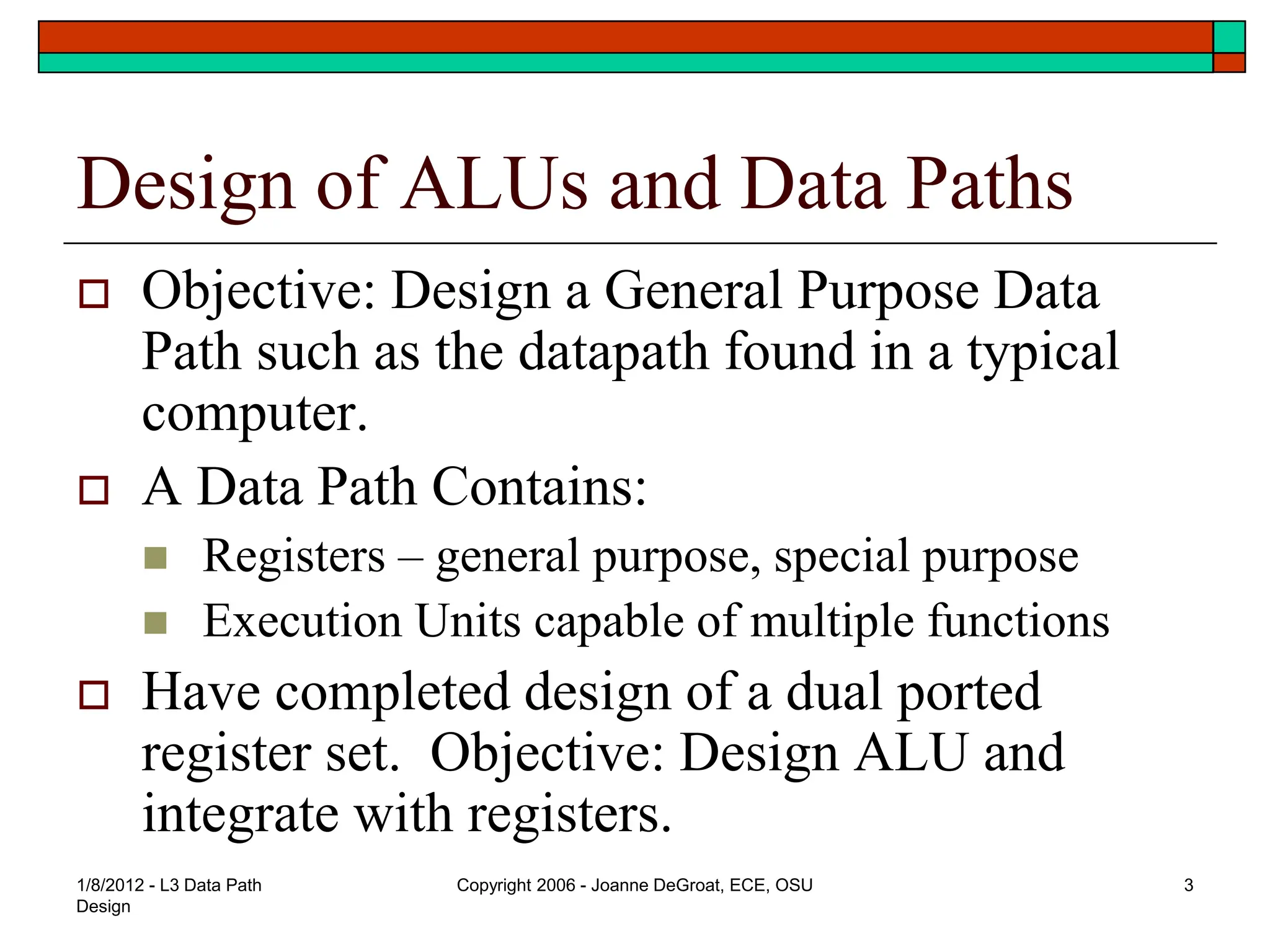
Design of ALUs and Data Paths
 Objective: Design a General Purpose Data
Path such as the datapath found in a typical
computer.
 A Data Path Contains:
 Registers – general purpose, special purpose
 Execution Units capable of multiple functions
 Have completed design of a dual ported
register set. Objective: Design ALU and
integrate with registers.
1/8/2012 - L3 Data Path
Design
Copyright 2006 - Joanne DeGroat, ECE, OSU 4
ALU Operations (integer ALU)
 Add (A+B)
 Add with Carry (A+B+Cin)
 Subtract (A-B)
 Subtract with Borrow (A-B-Cin)
 [Subract reverse (B-A)]
 [Subract reverse with Borrow (B-A-Cin)]
 Negative A (-A)
 Negative B (-B)
 Increment A (A+1)
 Increment B (B+1)
 Decrement A (A-1)
 Decrement B (B-1)
 Logical AND
 Logical OR
 Logical XOR
 Not A
 Not B
 A
 B
 Multiply Step or Multiply
 Divide Step or Divide
 Mask
 Conditional AND/OR (uses
Mask)
 Shift
 Zero
1/8/2012 - L3 Data Path
Design
Copyright 2006 - Joanne DeGroat, ECE, OSU 5
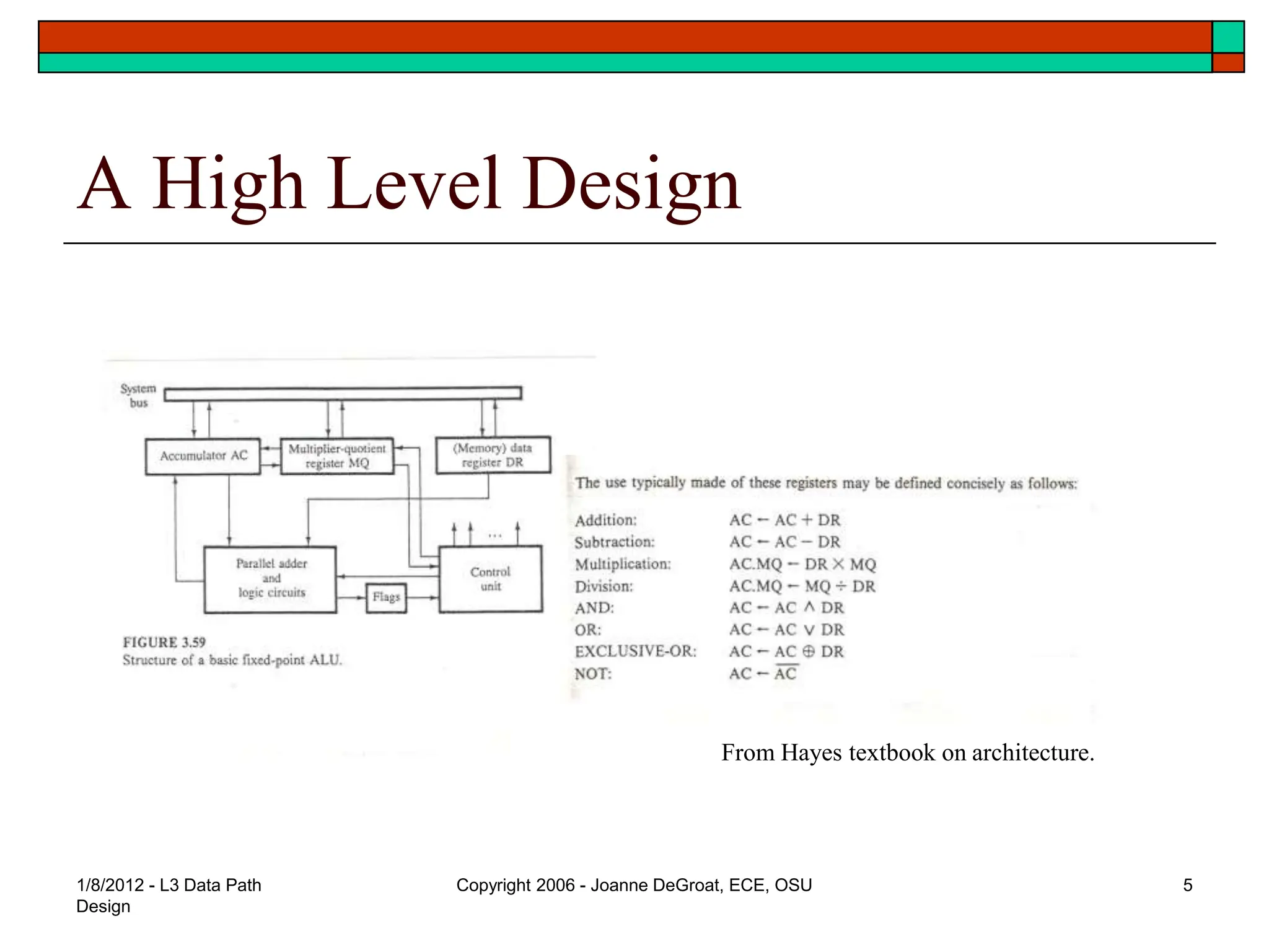
A High Level Design
From Hayes textbook on architecture.
1/8/2012 - L3 Data Path
Design
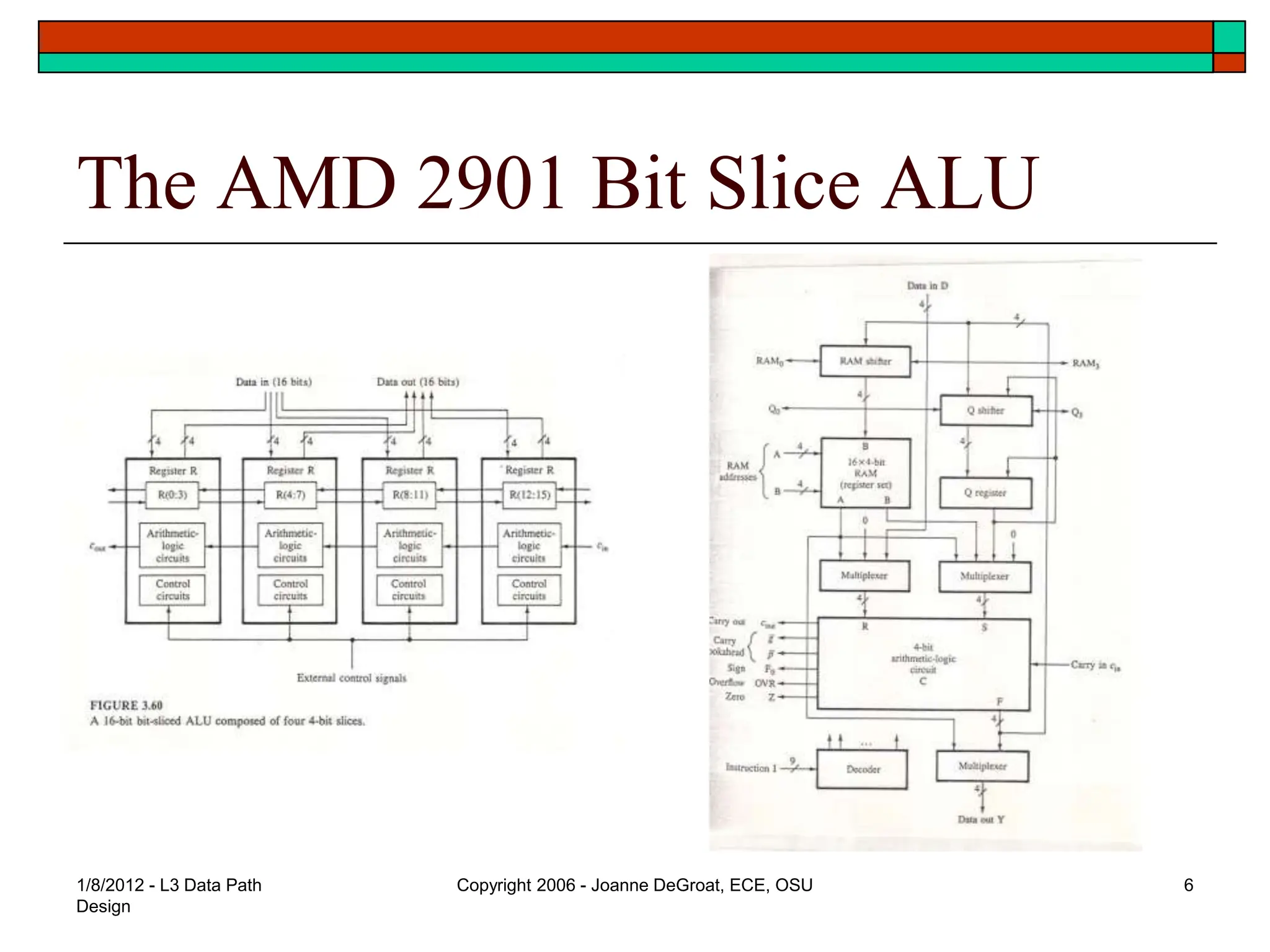
Copyright 2006 - Joanne DeGroat, ECE, OSU 6
The AMD 2901 Bit Slice ALU
1/8/2012 - L3 Data Path
Design
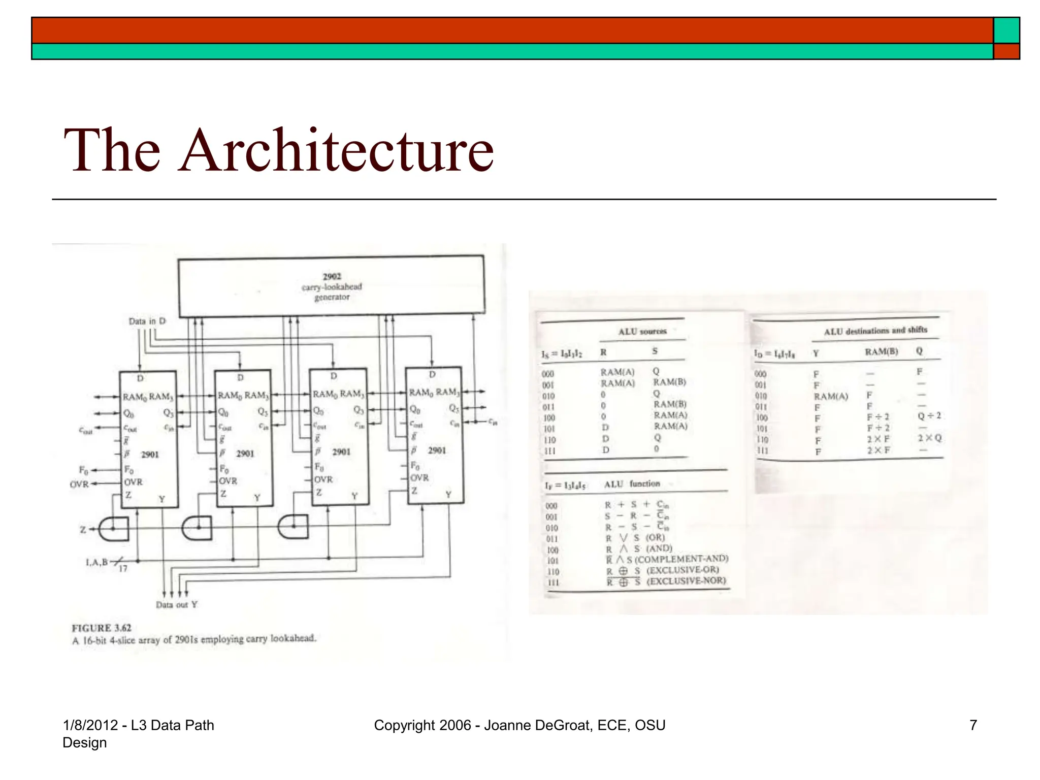
Copyright 2006 - Joanne DeGroat, ECE, OSU 7
The Architecture
1/8/2012 - L3 Data Path
Design
Copyright 2006 - Joanne DeGroat, ECE, OSU 8
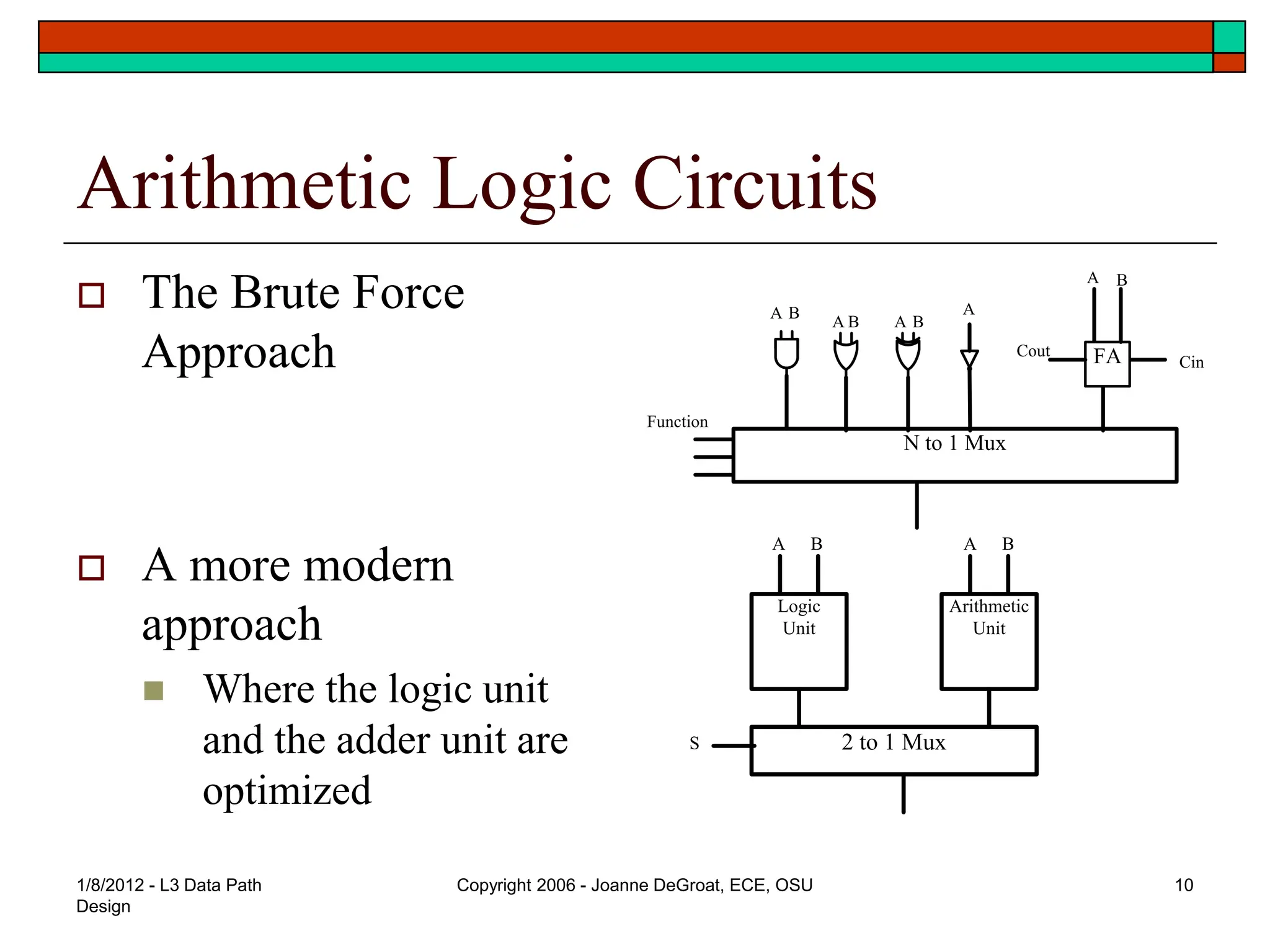
Arithmetic Logic Circuits
 The Brute Force Approach
 A more modern approach
1/8/2012 - L3 Data Path
Design
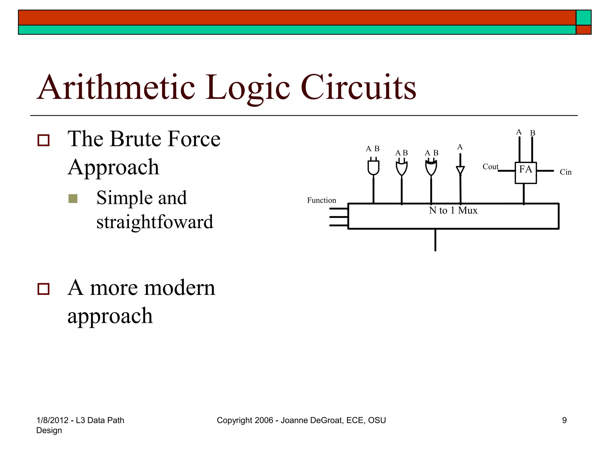
Copyright 2006 - Joanne DeGroat, ECE, OSU 9
Arithmetic Logic Circuits
 The Brute Force
Approach
 Simple and
straightfoward
 A more modern
approach
N to 1 Mux
FA
Function
Cout
Cin
A B
A A
A
A B
B
B
1/8/2012 - L3 Data Path
Design
Copyright 2006 - Joanne DeGroat, ECE, OSU 10
Arithmetic Logic Circuits
 The Brute Force
Approach
 A more modern
approach
 Where the logic unit
and the adder unit are
optimized
N to 1 Mux
FA
Function
Cout
Cin
A B
A A
A
A B
B
B
Logic
Unit
Arithmetic
Unit
2 to 1 Mux
A A
B B
S
1/8/2012 - L3 Data Path
Design
Copyright 2006 - Joanne DeGroat, ECE, OSU 11
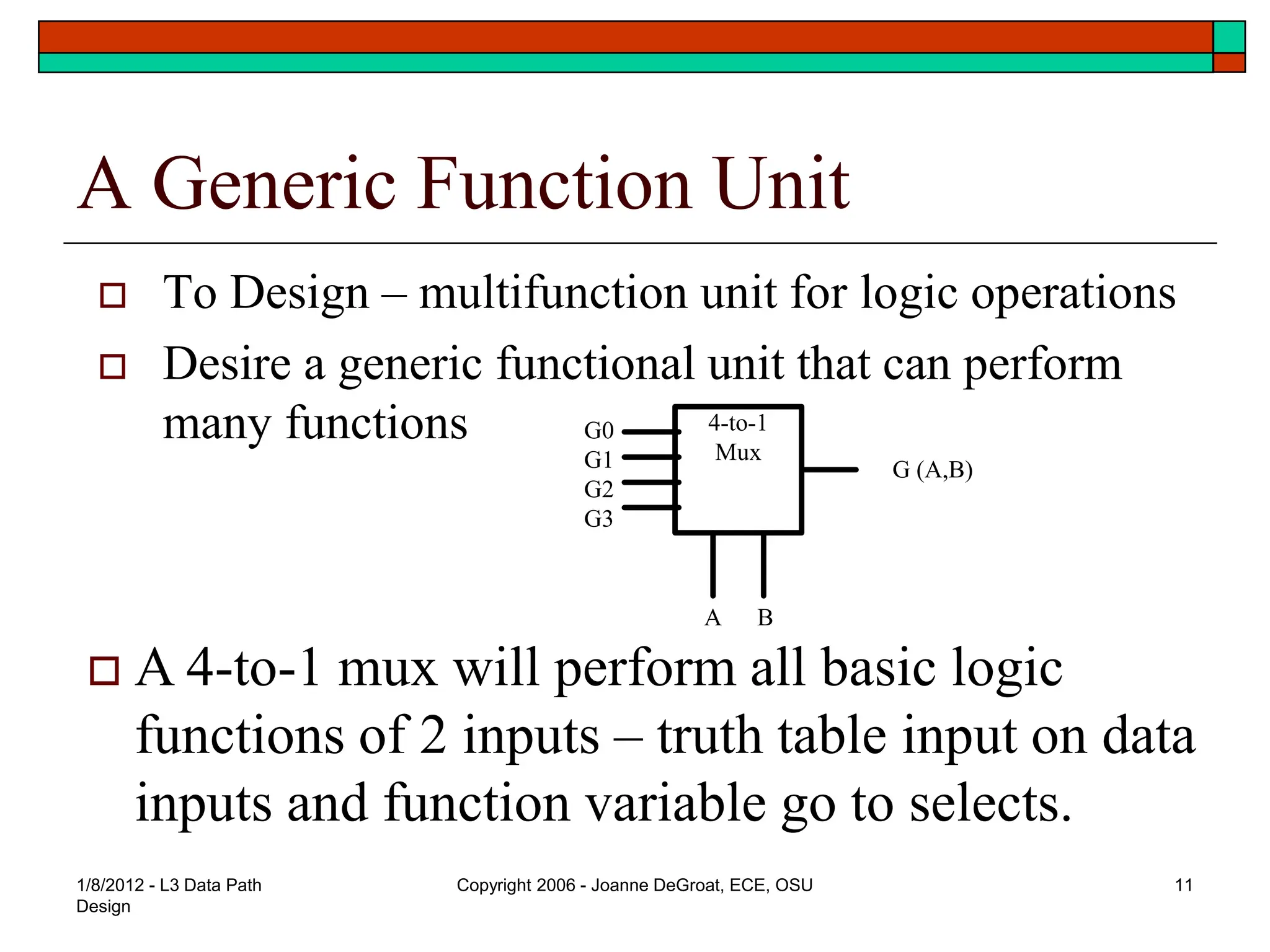
A Generic Function Unit
 To Design – multifunction unit for logic operations
 Desire a generic functional unit that can perform
many functions
 A 4-to-1 mux will perform all basic logic
functions of 2 inputs – truth table input on data
inputs and function variable go to selects.
G (A,B)
B
A
4-to-1
Mux
G0
G1
G2
G3
1/8/2012 - L3 Data Path
Design
Copyright 2006 - Joanne DeGroat, ECE, OSU 12
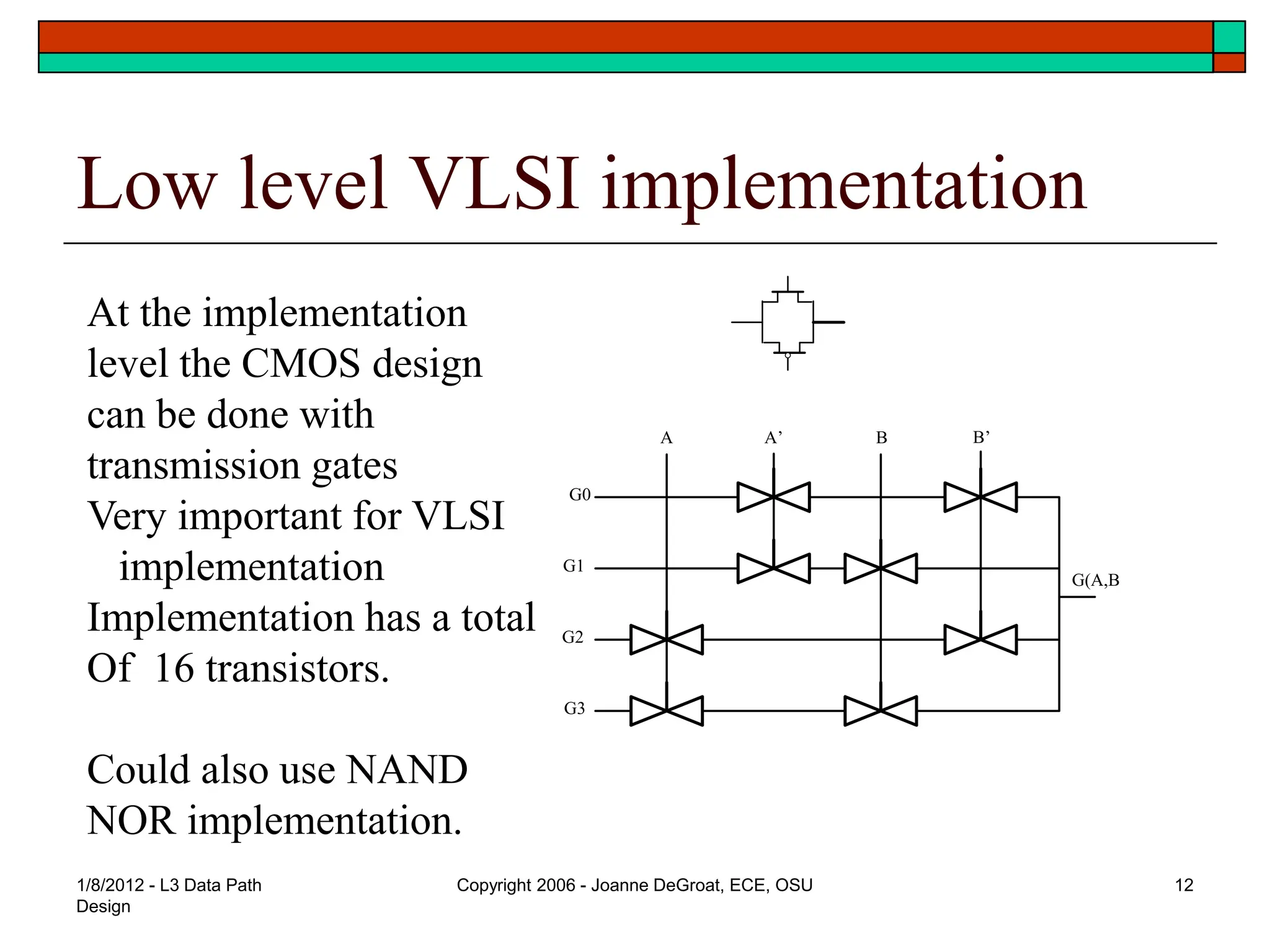
Low level VLSI implementation
G0
G1
G2
G3
A B B’
A’
G(A,B
At the implementation
level the CMOS design
can be done with
transmission gates
Very important for VLSI
implementation
Implementation has a total
Of 16 transistors.
Could also use NAND
NOR implementation.
1/8/2012 - L3 Data Path
Design
Copyright 2006 - Joanne DeGroat, ECE, OSU 13
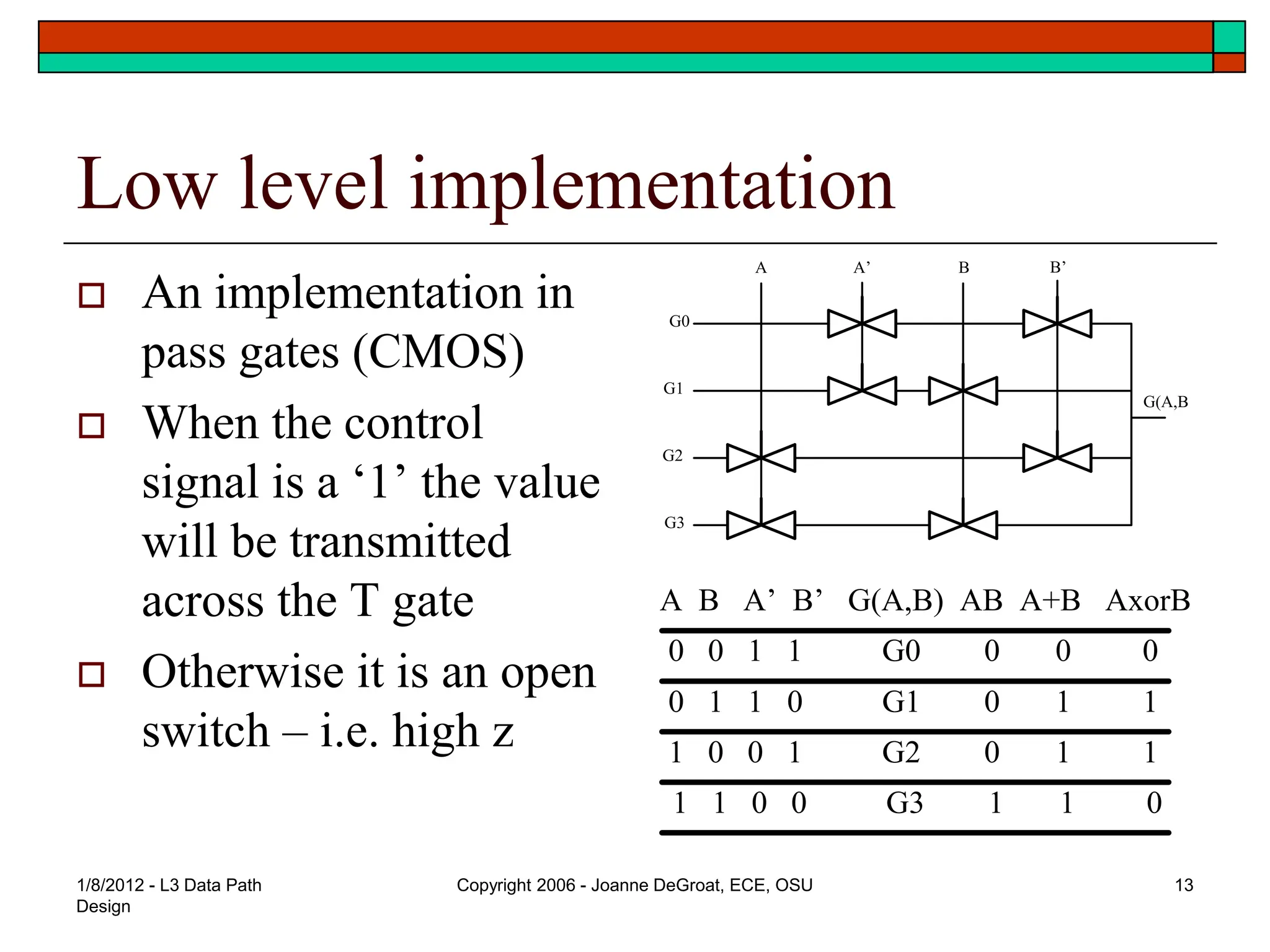
Low level implementation
 An implementation in
pass gates (CMOS)
 When the control
signal is a ‘1’ the value
will be transmitted
across the T gate
 Otherwise it is an open
switch – i.e. high z
G0
G1
G2
G3
A B B’
A’
G(A,B
A B A’ B’ G(A,B) AB A+B AxorB
0 0 1 1 G0 0 0 0
0 1 1 0 G1 0 1 1
1 0 0 1 G2 0 1 1
1 1 0 0 G3 1 1 0
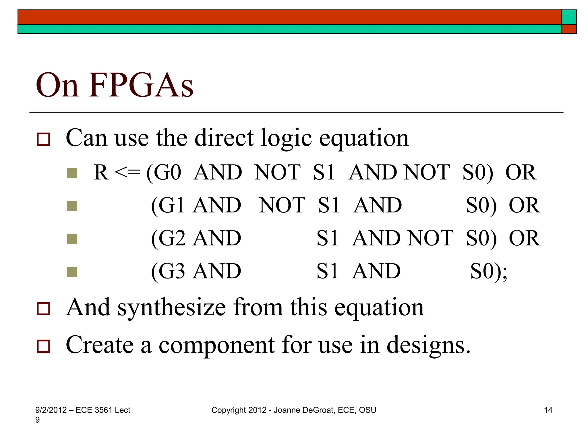
On FPGAs
 Can use the direct logic equation
 R <= (G0 AND NOT S1 AND NOT S0) OR
 (G1 AND NOT S1 AND S0) OR
 (G2 AND S1 AND NOT S0) OR
 (G3 AND S1 AND S0);
 And synthesize from this equation
 Create a component for use in designs.
9/2/2012 – ECE 3561 Lect
9
Copyright 2012 - Joanne DeGroat, ECE, OSU 14
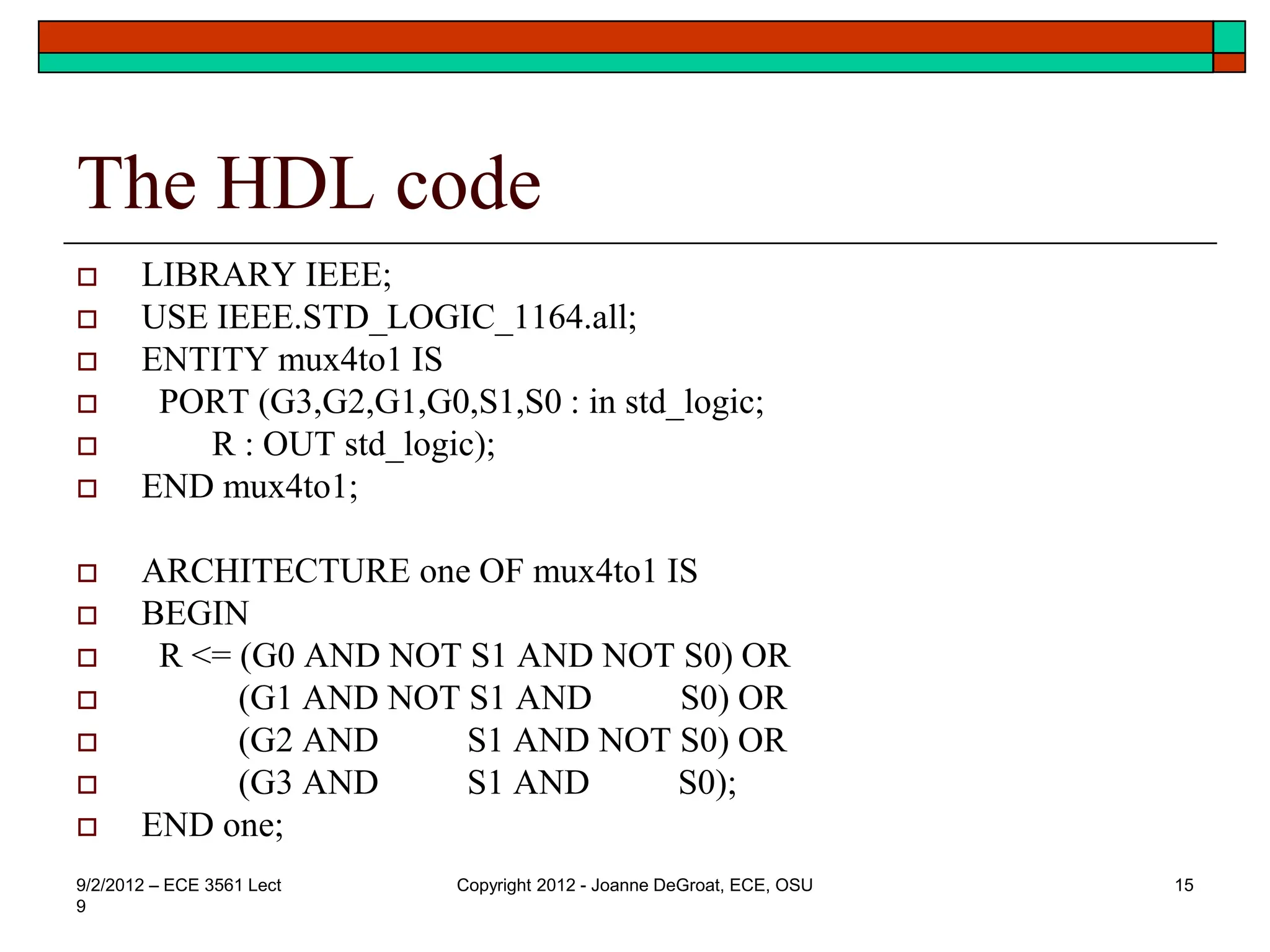
The HDL code
 LIBRARY IEEE;
 USE IEEE.STD_LOGIC_1164.all;
 ENTITY mux4to1 IS
 PORT (G3,G2,G1,G0,S1,S0 : in std_logic;
 R : OUT std_logic);
 END mux4to1;
 ARCHITECTURE one OF mux4to1 IS
 BEGIN
 R <= (G0 AND NOT S1 AND NOT S0) OR
 (G1 AND NOT S1 AND S0) OR
 (G2 AND S1 AND NOT S0) OR
 (G3 AND S1 AND S0);
 END one;
9/2/2012 – ECE 3561 Lect
9
Copyright 2012 - Joanne DeGroat, ECE, OSU 15
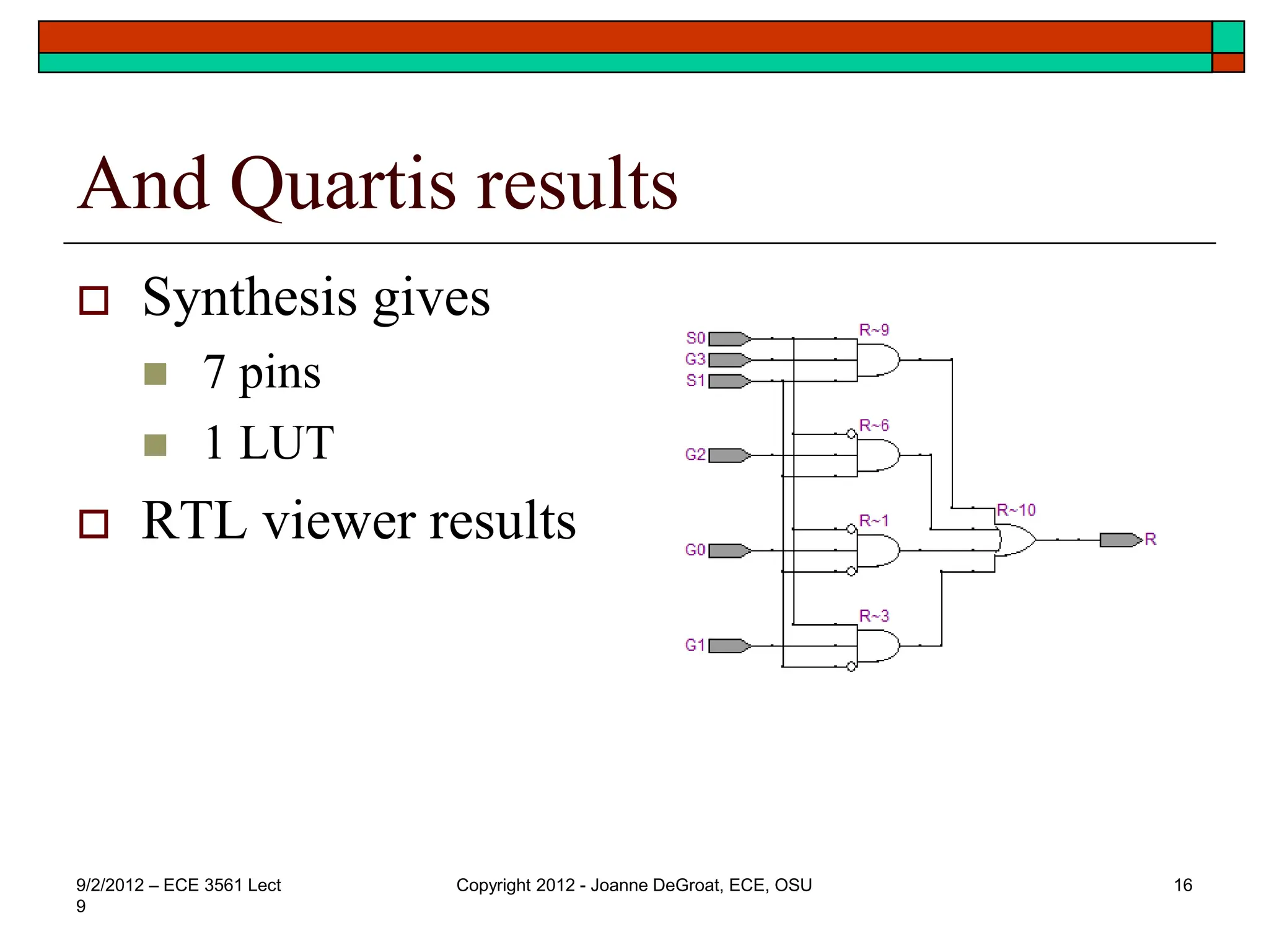
And Quartis results
 Synthesis gives
 7 pins
 1 LUT
 RTL viewer results
9/2/2012 – ECE 3561 Lect
9
Copyright 2012 - Joanne DeGroat, ECE, OSU 16
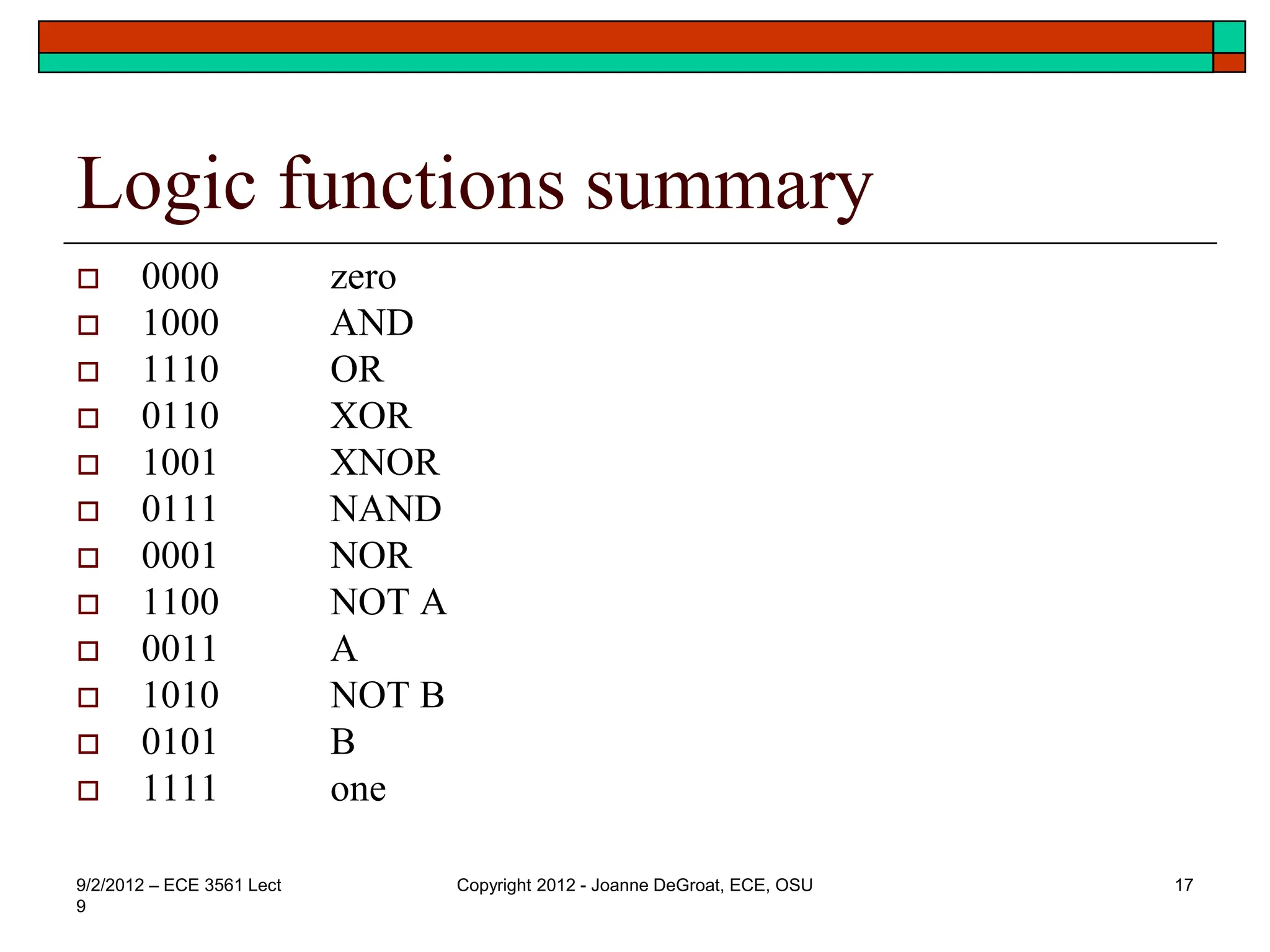
Logic functions summary
 0000 zero
 1000 AND
 1110 OR
 0110 XOR
 1001 XNOR
 0111 NAND
 0001 NOR
 1100 NOT A
 0011 A
 1010 NOT B
 0101 B
 1111 one
9/2/2012 – ECE 3561 Lect
9
Copyright 2012 - Joanne DeGroat, ECE, OSU 17
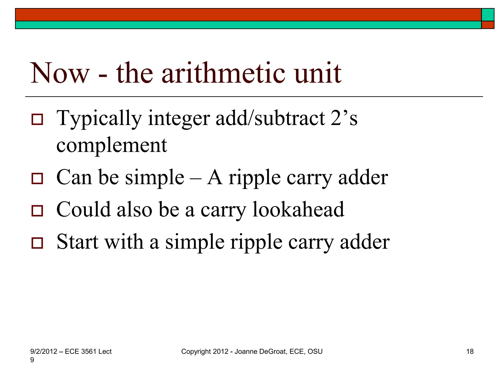
Now - the arithmetic unit
 Typically integer add/subtract 2’s
complement
 Can be simple – A ripple carry adder
 Could also be a carry lookahead
 Start with a simple ripple carry adder
9/2/2012 – ECE 3561 Lect
9
Copyright 2012 - Joanne DeGroat, ECE, OSU 18
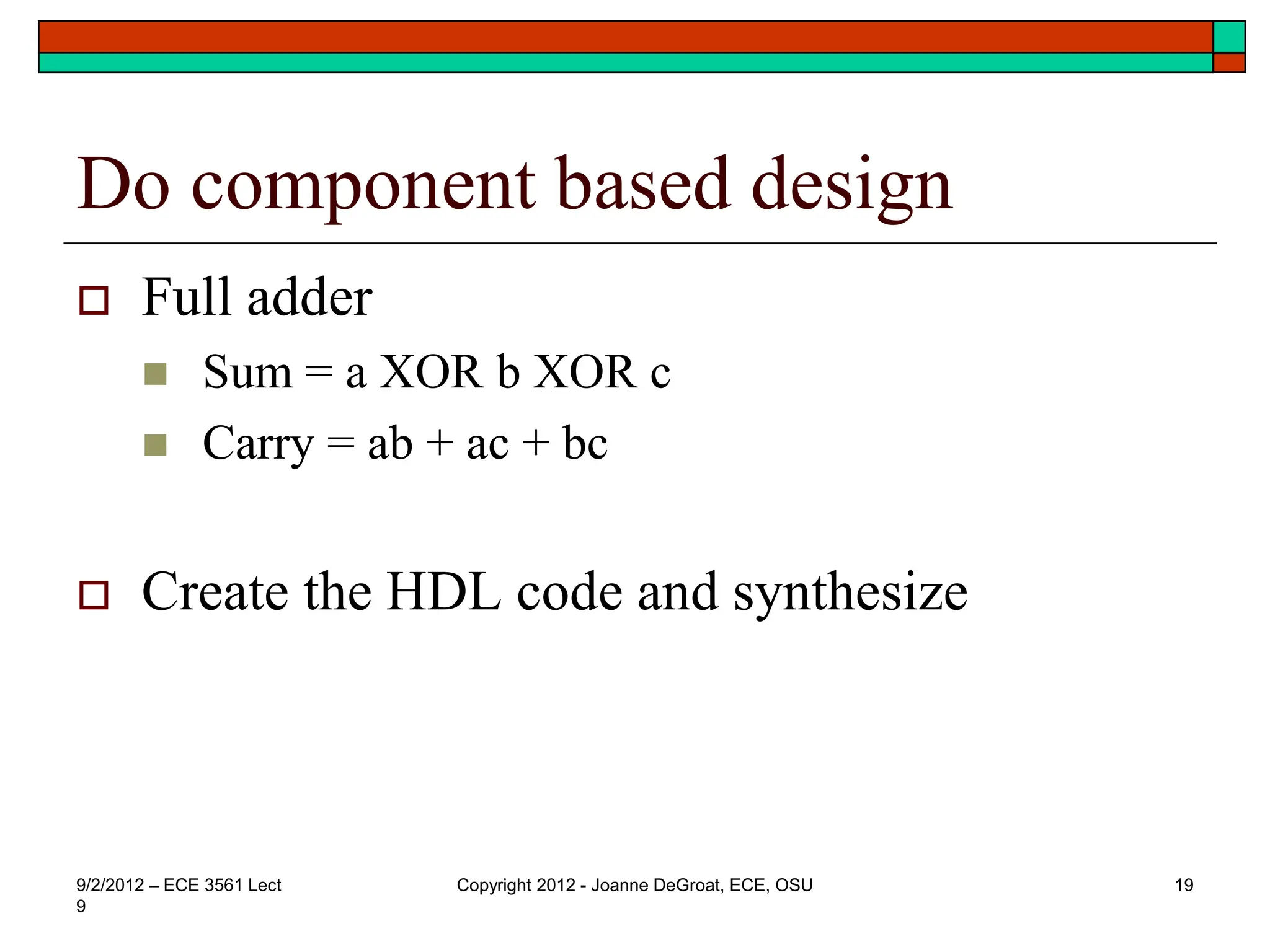
Do component based design
 Full adder
 Sum = a XOR b XOR c
 Carry = ab + ac + bc
 Create the HDL code and synthesize
9/2/2012 – ECE 3561 Lect
9
Copyright 2012 - Joanne DeGroat, ECE, OSU 19
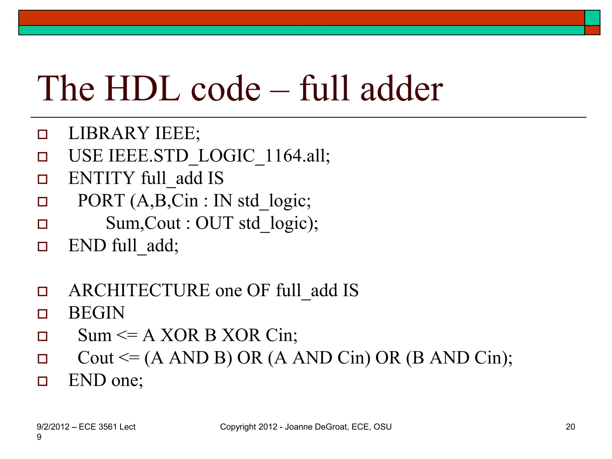
The HDL code – full adder
 LIBRARY IEEE;
 USE IEEE.STD_LOGIC_1164.all;
 ENTITY full_add IS
 PORT (A,B,Cin : IN std_logic;
 Sum,Cout : OUT std_logic);
 END full_add;
 ARCHITECTURE one OF full_add IS
 BEGIN
 Sum <= A XOR B XOR Cin;
 Cout <= (A AND B) OR (A AND Cin) OR (B AND Cin);
 END one;
9/2/2012 – ECE 3561 Lect
9
Copyright 2012 - Joanne DeGroat, ECE, OSU 20
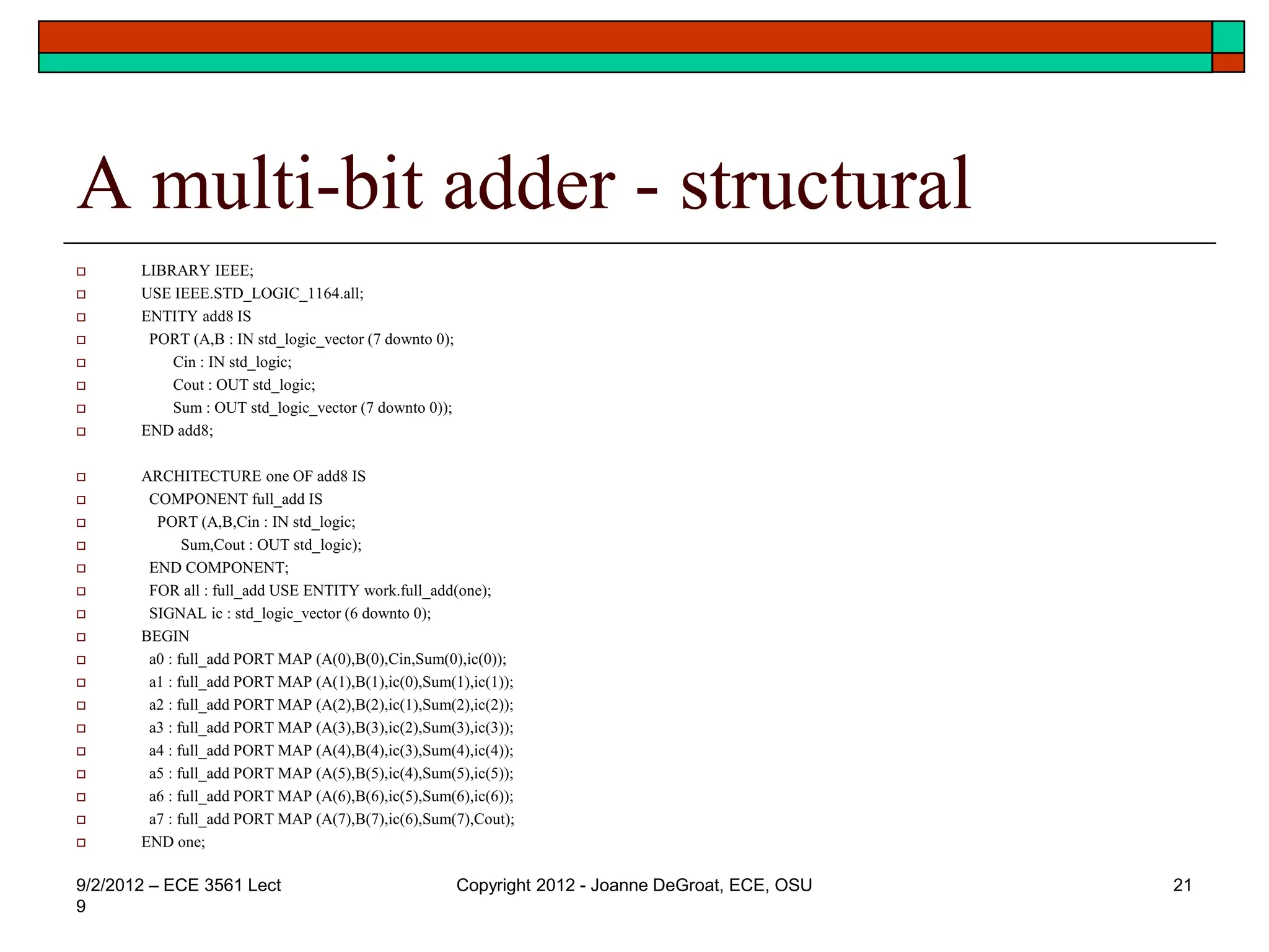
A multi-bit adder - structural
 LIBRARY IEEE;
 USE IEEE.STD_LOGIC_1164.all;
 ENTITY add8 IS
 PORT (A,B : IN std_logic_vector (7 downto 0);
 Cin : IN std_logic;
 Cout : OUT std_logic;
 Sum : OUT std_logic_vector (7 downto 0));
 END add8;
 ARCHITECTURE one OF add8 IS
 COMPONENT full_add IS
 PORT (A,B,Cin : IN std_logic;
 Sum,Cout : OUT std_logic);
 END COMPONENT;
 FOR all : full_add USE ENTITY work.full_add(one);
 SIGNAL ic : std_logic_vector (6 downto 0);
 BEGIN
 a0 : full_add PORT MAP (A(0),B(0),Cin,Sum(0),ic(0));
 a1 : full_add PORT MAP (A(1),B(1),ic(0),Sum(1),ic(1));
 a2 : full_add PORT MAP (A(2),B(2),ic(1),Sum(2),ic(2));
 a3 : full_add PORT MAP (A(3),B(3),ic(2),Sum(3),ic(3));
 a4 : full_add PORT MAP (A(4),B(4),ic(3),Sum(4),ic(4));
 a5 : full_add PORT MAP (A(5),B(5),ic(4),Sum(5),ic(5));
 a6 : full_add PORT MAP (A(6),B(6),ic(5),Sum(6),ic(6));
 a7 : full_add PORT MAP (A(7),B(7),ic(6),Sum(7),Cout);
 END one;
9/2/2012 – ECE 3561 Lect
9
Copyright 2012 - Joanne DeGroat, ECE, OSU 21
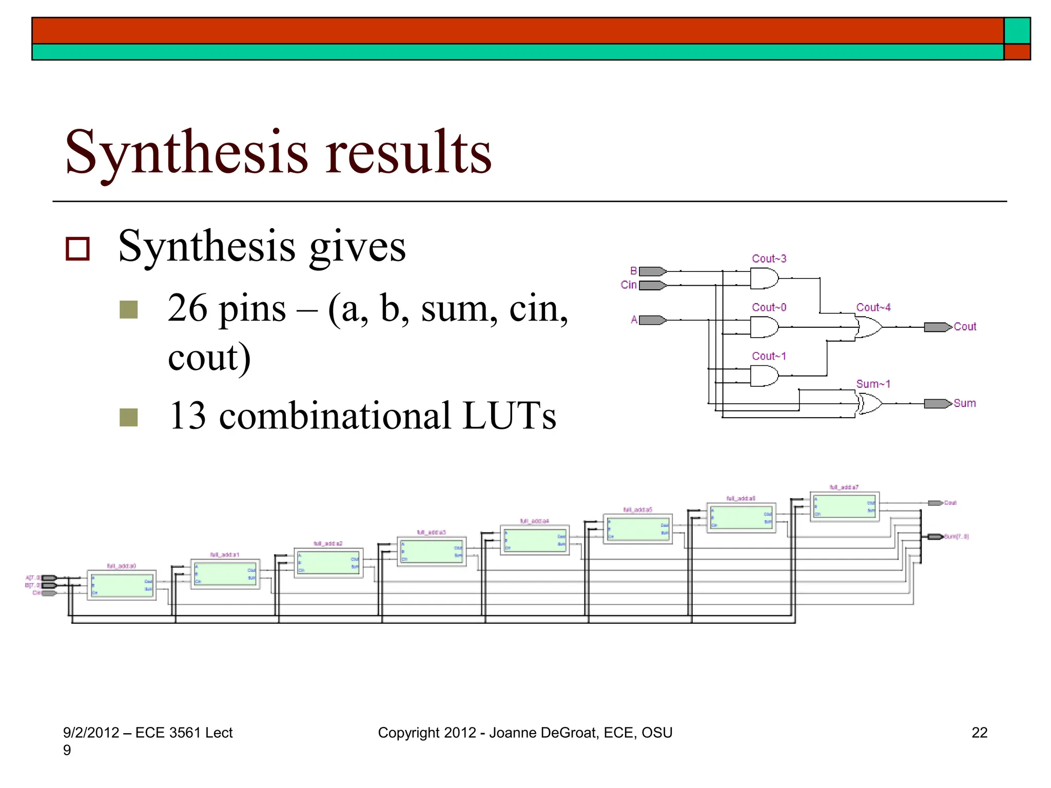
Synthesis results
 Synthesis gives
 26 pins – (a, b, sum, cin,
cout)
 13 combinational LUTs
9/2/2012 – ECE 3561 Lect
9
Copyright 2012 - Joanne DeGroat, ECE, OSU 22
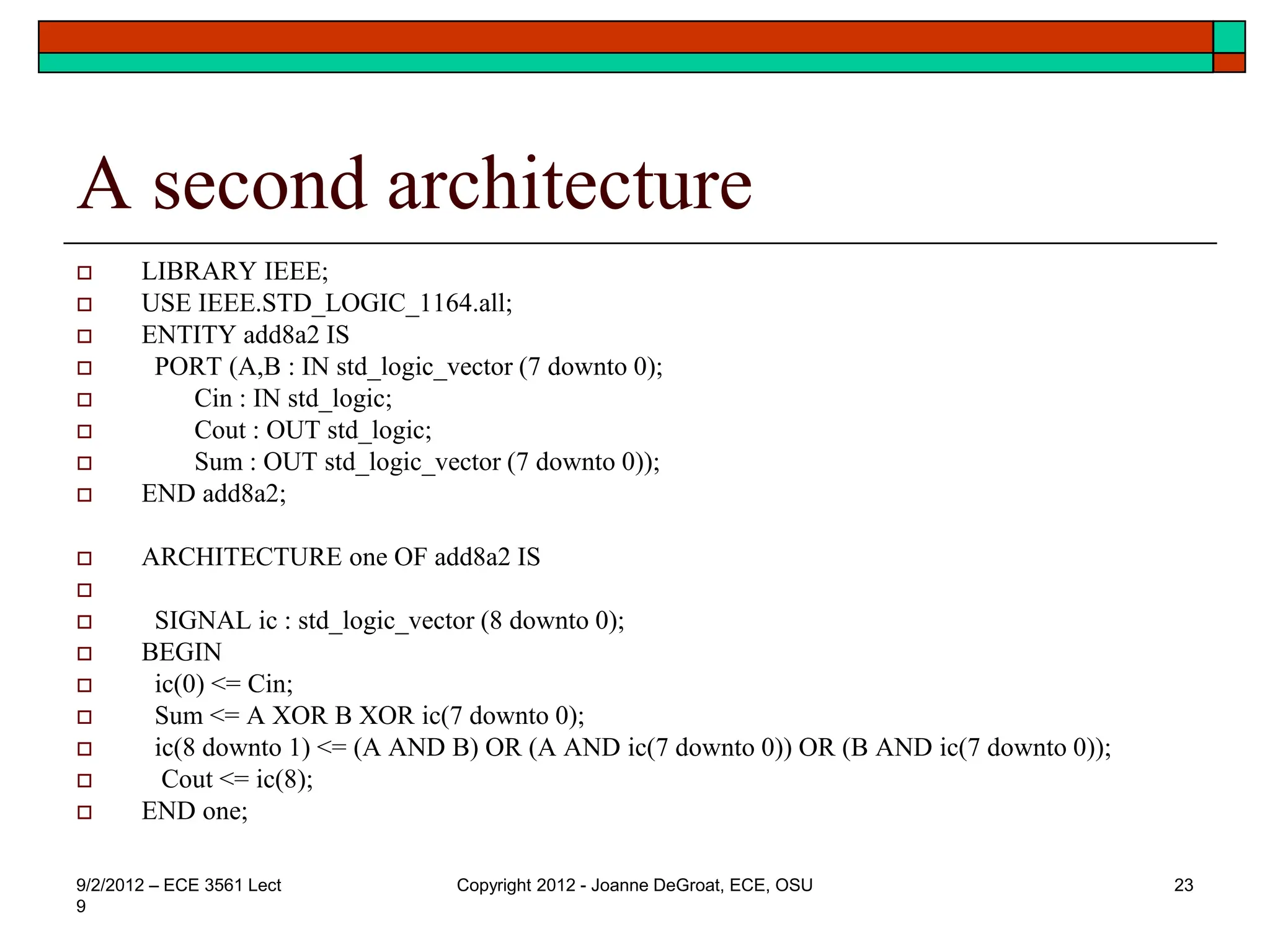
A second architecture
 LIBRARY IEEE;
 USE IEEE.STD_LOGIC_1164.all;
 ENTITY add8a2 IS
 PORT (A,B : IN std_logic_vector (7 downto 0);
 Cin : IN std_logic;
 Cout : OUT std_logic;
 Sum : OUT std_logic_vector (7 downto 0));
 END add8a2;
 ARCHITECTURE one OF add8a2 IS

 SIGNAL ic : std_logic_vector (8 downto 0);
 BEGIN
 ic(0) <= Cin;
 Sum <= A XOR B XOR ic(7 downto 0);
 ic(8 downto 1) <= (A AND B) OR (A AND ic(7 downto 0)) OR (B AND ic(7 downto 0));
 Cout <= ic(8);
 END one;
9/2/2012 – ECE 3561 Lect
9
Copyright 2012 - Joanne DeGroat, ECE, OSU 23
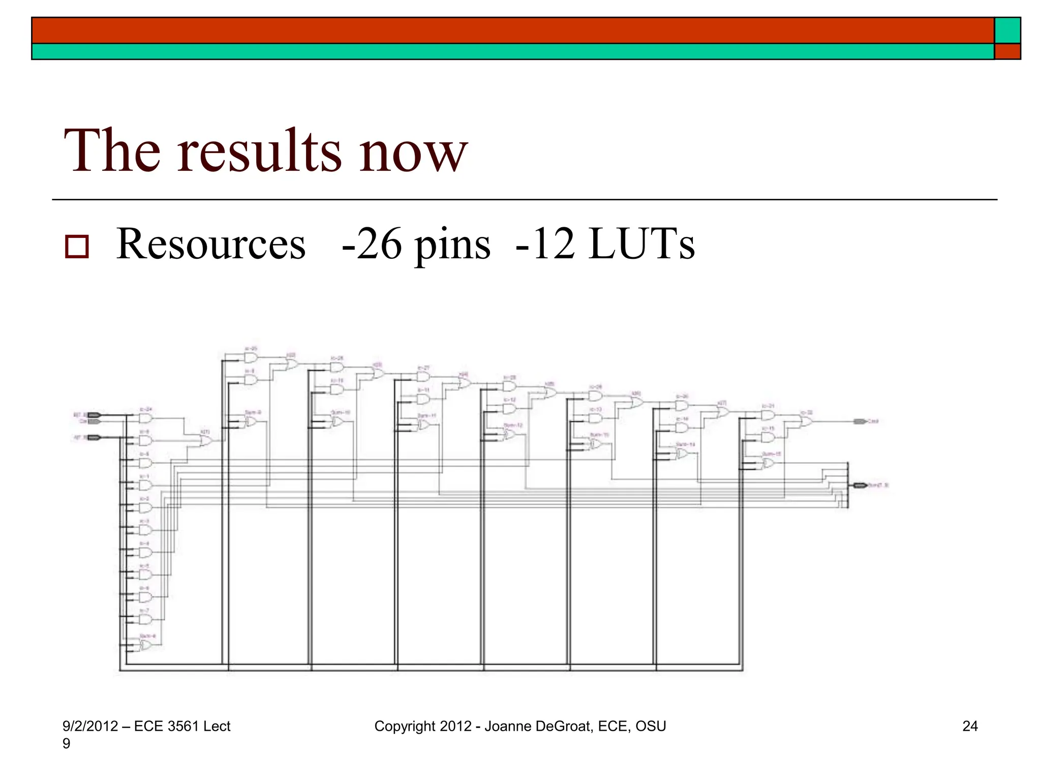
The results now
 Resources -26 pins -12 LUTs
9/2/2012 – ECE 3561 Lect
9
Copyright 2012 - Joanne DeGroat, ECE, OSU 24
Lecture summary
 The adder was a simple ripple carry adder.
 Other Architectures
 Carry Lookahead
 Carry select
 Carry multiplexed
9/2/2012 – ECE 3561 Lect
9
Copyright 2012 - Joanne DeGroat, ECE, OSU 25

ECE 3561 - Lecture 23 Arithmetic Logic Units.ppt

  • 1.
    L23 – ArithmeticLogic Units
  • 2.
    Arithmetic Logic Units(ALU)  Modern ALU design  ALU is heart of datapath  Ref: text Unit 15 9/2/2012 – ECE 3561 Lect 9 Copyright 2012 - Joanne DeGroat, ECE, OSU 2
  • 3.
    1/8/2012 - L3Data Path Design Copyright 2006 - Joanne DeGroat, ECE, OSU 3 Design of ALUs and Data Paths  Objective: Design a General Purpose Data Path such as the datapath found in a typical computer.  A Data Path Contains:  Registers – general purpose, special purpose  Execution Units capable of multiple functions  Have completed design of a dual ported register set. Objective: Design ALU and integrate with registers.
  • 4.
    1/8/2012 - L3Data Path Design Copyright 2006 - Joanne DeGroat, ECE, OSU 4 ALU Operations (integer ALU)  Add (A+B)  Add with Carry (A+B+Cin)  Subtract (A-B)  Subtract with Borrow (A-B-Cin)  [Subract reverse (B-A)]  [Subract reverse with Borrow (B-A-Cin)]  Negative A (-A)  Negative B (-B)  Increment A (A+1)  Increment B (B+1)  Decrement A (A-1)  Decrement B (B-1)  Logical AND  Logical OR  Logical XOR  Not A  Not B  A  B  Multiply Step or Multiply  Divide Step or Divide  Mask  Conditional AND/OR (uses Mask)  Shift  Zero
  • 5.
    1/8/2012 - L3Data Path Design Copyright 2006 - Joanne DeGroat, ECE, OSU 5 A High Level Design From Hayes textbook on architecture.
  • 6.
    1/8/2012 - L3Data Path Design Copyright 2006 - Joanne DeGroat, ECE, OSU 6 The AMD 2901 Bit Slice ALU
  • 7.
    1/8/2012 - L3Data Path Design Copyright 2006 - Joanne DeGroat, ECE, OSU 7 The Architecture
  • 8.
    1/8/2012 - L3Data Path Design Copyright 2006 - Joanne DeGroat, ECE, OSU 8 Arithmetic Logic Circuits  The Brute Force Approach  A more modern approach
  • 9.
    1/8/2012 - L3Data Path Design Copyright 2006 - Joanne DeGroat, ECE, OSU 9 Arithmetic Logic Circuits  The Brute Force Approach  Simple and straightfoward  A more modern approach N to 1 Mux FA Function Cout Cin A B A A A A B B B
  • 10.
    1/8/2012 - L3Data Path Design Copyright 2006 - Joanne DeGroat, ECE, OSU 10 Arithmetic Logic Circuits  The Brute Force Approach  A more modern approach  Where the logic unit and the adder unit are optimized N to 1 Mux FA Function Cout Cin A B A A A A B B B Logic Unit Arithmetic Unit 2 to 1 Mux A A B B S
  • 11.
    1/8/2012 - L3Data Path Design Copyright 2006 - Joanne DeGroat, ECE, OSU 11 A Generic Function Unit  To Design – multifunction unit for logic operations  Desire a generic functional unit that can perform many functions  A 4-to-1 mux will perform all basic logic functions of 2 inputs – truth table input on data inputs and function variable go to selects. G (A,B) B A 4-to-1 Mux G0 G1 G2 G3
  • 12.
    1/8/2012 - L3Data Path Design Copyright 2006 - Joanne DeGroat, ECE, OSU 12 Low level VLSI implementation G0 G1 G2 G3 A B B’ A’ G(A,B At the implementation level the CMOS design can be done with transmission gates Very important for VLSI implementation Implementation has a total Of 16 transistors. Could also use NAND NOR implementation.
  • 13.
    1/8/2012 - L3Data Path Design Copyright 2006 - Joanne DeGroat, ECE, OSU 13 Low level implementation  An implementation in pass gates (CMOS)  When the control signal is a ‘1’ the value will be transmitted across the T gate  Otherwise it is an open switch – i.e. high z G0 G1 G2 G3 A B B’ A’ G(A,B A B A’ B’ G(A,B) AB A+B AxorB 0 0 1 1 G0 0 0 0 0 1 1 0 G1 0 1 1 1 0 0 1 G2 0 1 1 1 1 0 0 G3 1 1 0
  • 14.
    On FPGAs  Canuse the direct logic equation  R <= (G0 AND NOT S1 AND NOT S0) OR  (G1 AND NOT S1 AND S0) OR  (G2 AND S1 AND NOT S0) OR  (G3 AND S1 AND S0);  And synthesize from this equation  Create a component for use in designs. 9/2/2012 – ECE 3561 Lect 9 Copyright 2012 - Joanne DeGroat, ECE, OSU 14
  • 15.
    The HDL code LIBRARY IEEE;  USE IEEE.STD_LOGIC_1164.all;  ENTITY mux4to1 IS  PORT (G3,G2,G1,G0,S1,S0 : in std_logic;  R : OUT std_logic);  END mux4to1;  ARCHITECTURE one OF mux4to1 IS  BEGIN  R <= (G0 AND NOT S1 AND NOT S0) OR  (G1 AND NOT S1 AND S0) OR  (G2 AND S1 AND NOT S0) OR  (G3 AND S1 AND S0);  END one; 9/2/2012 – ECE 3561 Lect 9 Copyright 2012 - Joanne DeGroat, ECE, OSU 15
  • 16.
    And Quartis results Synthesis gives  7 pins  1 LUT  RTL viewer results 9/2/2012 – ECE 3561 Lect 9 Copyright 2012 - Joanne DeGroat, ECE, OSU 16
  • 17.
    Logic functions summary 0000 zero  1000 AND  1110 OR  0110 XOR  1001 XNOR  0111 NAND  0001 NOR  1100 NOT A  0011 A  1010 NOT B  0101 B  1111 one 9/2/2012 – ECE 3561 Lect 9 Copyright 2012 - Joanne DeGroat, ECE, OSU 17
  • 18.
    Now - thearithmetic unit  Typically integer add/subtract 2’s complement  Can be simple – A ripple carry adder  Could also be a carry lookahead  Start with a simple ripple carry adder 9/2/2012 – ECE 3561 Lect 9 Copyright 2012 - Joanne DeGroat, ECE, OSU 18
  • 19.
    Do component baseddesign  Full adder  Sum = a XOR b XOR c  Carry = ab + ac + bc  Create the HDL code and synthesize 9/2/2012 – ECE 3561 Lect 9 Copyright 2012 - Joanne DeGroat, ECE, OSU 19
  • 20.
    The HDL code– full adder  LIBRARY IEEE;  USE IEEE.STD_LOGIC_1164.all;  ENTITY full_add IS  PORT (A,B,Cin : IN std_logic;  Sum,Cout : OUT std_logic);  END full_add;  ARCHITECTURE one OF full_add IS  BEGIN  Sum <= A XOR B XOR Cin;  Cout <= (A AND B) OR (A AND Cin) OR (B AND Cin);  END one; 9/2/2012 – ECE 3561 Lect 9 Copyright 2012 - Joanne DeGroat, ECE, OSU 20
  • 21.
    A multi-bit adder- structural  LIBRARY IEEE;  USE IEEE.STD_LOGIC_1164.all;  ENTITY add8 IS  PORT (A,B : IN std_logic_vector (7 downto 0);  Cin : IN std_logic;  Cout : OUT std_logic;  Sum : OUT std_logic_vector (7 downto 0));  END add8;  ARCHITECTURE one OF add8 IS  COMPONENT full_add IS  PORT (A,B,Cin : IN std_logic;  Sum,Cout : OUT std_logic);  END COMPONENT;  FOR all : full_add USE ENTITY work.full_add(one);  SIGNAL ic : std_logic_vector (6 downto 0);  BEGIN  a0 : full_add PORT MAP (A(0),B(0),Cin,Sum(0),ic(0));  a1 : full_add PORT MAP (A(1),B(1),ic(0),Sum(1),ic(1));  a2 : full_add PORT MAP (A(2),B(2),ic(1),Sum(2),ic(2));  a3 : full_add PORT MAP (A(3),B(3),ic(2),Sum(3),ic(3));  a4 : full_add PORT MAP (A(4),B(4),ic(3),Sum(4),ic(4));  a5 : full_add PORT MAP (A(5),B(5),ic(4),Sum(5),ic(5));  a6 : full_add PORT MAP (A(6),B(6),ic(5),Sum(6),ic(6));  a7 : full_add PORT MAP (A(7),B(7),ic(6),Sum(7),Cout);  END one; 9/2/2012 – ECE 3561 Lect 9 Copyright 2012 - Joanne DeGroat, ECE, OSU 21
  • 22.
    Synthesis results  Synthesisgives  26 pins – (a, b, sum, cin, cout)  13 combinational LUTs 9/2/2012 – ECE 3561 Lect 9 Copyright 2012 - Joanne DeGroat, ECE, OSU 22
  • 23.
    A second architecture LIBRARY IEEE;  USE IEEE.STD_LOGIC_1164.all;  ENTITY add8a2 IS  PORT (A,B : IN std_logic_vector (7 downto 0);  Cin : IN std_logic;  Cout : OUT std_logic;  Sum : OUT std_logic_vector (7 downto 0));  END add8a2;  ARCHITECTURE one OF add8a2 IS   SIGNAL ic : std_logic_vector (8 downto 0);  BEGIN  ic(0) <= Cin;  Sum <= A XOR B XOR ic(7 downto 0);  ic(8 downto 1) <= (A AND B) OR (A AND ic(7 downto 0)) OR (B AND ic(7 downto 0));  Cout <= ic(8);  END one; 9/2/2012 – ECE 3561 Lect 9 Copyright 2012 - Joanne DeGroat, ECE, OSU 23
  • 24.
    The results now Resources -26 pins -12 LUTs 9/2/2012 – ECE 3561 Lect 9 Copyright 2012 - Joanne DeGroat, ECE, OSU 24
  • 25.
    Lecture summary  Theadder was a simple ripple carry adder.  Other Architectures  Carry Lookahead  Carry select  Carry multiplexed 9/2/2012 – ECE 3561 Lect 9 Copyright 2012 - Joanne DeGroat, ECE, OSU 25