Comprehensive Lecture Notes on Low Power VLSI Circuit Design and Techniques
Detailed exploration of low power VLSI fundamentals, power dissipation sources, design approaches, and low-voltage adders, multipliers, and memories for efficient integrated circuit design.
Comprehensive Lecture Notes on Low Power VLSI Circuit Design and Techniques
1.
1
INSTITUTE OF AERONAUTICALENGINEERING
(AUTONOMOUS)
Dundigal, Hyderabad - 500 043
LECTURE NOTES:
LOW POWER VLSI CIRCUITS(AECD53)
DRAFTED BY :
MR. V.PRASANNANJANEYAREDDY (IARE 11124)
Assistant Professor
DEPARTMENT OF ELECTRONICS AND COMMUNICATION ENGINEERING
INSTITUTE OF AERONAUTICAL ENGINEERING
June 11, 2026
2.
2
1. FUNDAMENTALS
1.1 Needfor Low Power Circuit Design
1.2 Sources of Power Dissipation – Switching Power Dissipation
1.3 Short Circuit Power Dissipation
1.4 Leakage Power Dissipation
1.5 Glitching Power Dissipation
1.6 Short Channel Effects – Drain Induced Barrier Lowering and Punch Through
1.7 Surface Scattering
1.8 Velocity Saturation
1.9 Impact Ionization
1.10 Hot Electron Effect.
2. LOW-POWER CIRCUIT DESIGN APPROACHES
2.1 Low-Power Design through Voltage Scaling – VTCMOS circuits
2.2 MTCMOS circuits
2.3 Architectural Level Approach –Pipelining and Parallel Processing Approaches
2.4 Switched Capacitance Minimization Approaches:
2.5 System Level Measures
2.6 Circuit Level Measures
2.7 Mask level Measures.
3. LOW VOLTAGE LOW POWER ADDER
3.1 Introduction
3.2 Standard Adder Cells
3.3 CMOS Adder’s Architectures – Ripple Carry Adders
3.4 Low-Voltage Low Power Design Techniques
3.5 Trends of Technology and Power Supply Voltage
3.6 Low-Voltage Low-Power Logic Styles.
3.
3
4. LOW-VOLTAGE LOW-POWERMULTIPLIERS
4.1 Introduction
4.2 Overview of Multiplication
4.3 Types of Multiplier Architectures
4.4 Braun Multiplier
4.5 Baugh Wooley Multiplier
4.6 Booth Multiplier.
5. LOW-VOLTAGE LOW-POWER MEMORIES
5.1 Basics of ROM
5.2 Low-Power ROM Technology
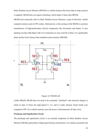
5.3 Basics of SRAM
5.4 Memory Cell
5.5 Precharge and Equalization Circuit
5.6 Low-Power SRAM Technologies
5.7 Basics of DRAM
5.8 Self-Refresh Circuit.
4.
4
MODULE I
FUNDAMENTALS
Course Outcomes
Aftersuccessful completion of this module, students should be able to:
CO1 Understand the basic need of low power VLSI circuits to reduce the
power dissipation
Understand
1.1. Need for Low Power Circuit Design
Low Power Circuit Design is one of the most important areas in modern Very Large-Scale
Integration (VLSI) systems. With the rapid advancement of semiconductor technology, the
number of transistors integrated onto a single chip has increased dramatically. Modern
integrated circuits used in smartphones, laptops, wearable devices, wireless communication
systems, medical implants, automotive electronics, and Internet of Things (IoT) applications
contain millions to billions of transistors. While this increase in transistor density has
significantly improved system performance and functionality, it has also resulted in higher
power consumption. Consequently, reducing power dissipation has become a major design
objective in VLSI circuits.
In earlier generations of integrated circuits, designers primarily focused on improving speed,
functionality, and chip area utilization. Power consumption was considered a secondary concern
because the number of transistors and operating frequencies were relatively low. However, as
CMOS technology scaled into deep submicron and nanometer regimes, power dissipation
emerged as a critical challenge. Today, low-power design is essential not only for portable
battery-operated devices but also for high-performance computing systems, servers, and data
centers where energy consumption significantly impacts operating costs and environmental
sustainability.
5.
5
The need forlow-power circuit design arises from several factors including battery limitations,
heat generation, reliability concerns, environmental issues, packaging constraints, and
technology scaling effects. Therefore, modern VLSI designers must carefully optimize circuits
to achieve the desired balance between performance and power consumption.
Battery Life Enhancement
One of the primary motivations for low-power circuit design is the increasing demand for
portable electronic devices. Smartphones, tablets, smartwatches, digital cameras, wireless
sensors, hearing aids, and medical implants depend on batteries as their primary source of
energy. The operating lifetime of these devices is directly determined by their power
consumption.
Consumers expect portable devices to operate for extended periods without frequent recharging.
For example, smartphone users expect a battery life of at least one full day despite intensive
usage involving communication, multimedia processing, internet browsing, and gaming.
Similarly, wearable devices such as fitness trackers and smartwatches require low-power
operation to maximize battery life while maintaining compact size.
Medical devices such as pacemakers and implanted monitoring systems present an even greater
challenge because battery replacement often requires surgical procedures. In such applications,
low-power circuit design is crucial for extending operational lifetime and reducing maintenance
requirements.
By minimizing power dissipation, designers can significantly extend battery life, improve user
convenience, and reduce overall operating costs. Therefore, low-power techniques have become
indispensable in portable electronic systems.
Reduction of Heat Generation
Power dissipation in integrated circuits ultimately converts electrical energy into heat. As
transistor density and operating frequencies increase, the amount of heat generated within a chip
also increases substantially. Excessive heat can lead to several problems including:
6.
6
Modern microprocessors andgraphics processors can dissipate hundreds of watts of power
during operation. Without proper thermal management, chip temperatures may exceed safe
operating limits, causing malfunction or failure.
Low-power circuit design reduces the amount of energy converted into heat. Lower operating
temperatures improve system stability and reliability while reducing the need for expensive
cooling solutions such as heat sinks, fans, liquid cooling systems, and thermal management
circuits.
In portable devices, reduced heat generation also improves user comfort and prevents
overheating during prolonged operation. Thus, minimizing power dissipation is essential for
maintaining acceptable thermal conditions in modern electronic systems.
Improved Reliability and Device Lifetime
Reliability is a critical consideration in integrated circuit design. High power dissipation
increases chip temperature, which accelerates various failure mechanisms including:
According to semiconductor reliability studies, even a small increase in operating
temperature can significantly reduce device lifetime. Elevated temperatures cause metal
interconnects to degrade more rapidly and increase defect generation within semiconductor
materials.
Low-power design helps maintain lower operating temperatures, thereby reducing thermal
stress and enhancing long-term reliability. This is especially important in mission-critical
applications such as aerospace systems, medical equipment, military electronics, and industrial
control systems where failures can have severe consequences.
By reducing power consumption, designers improve device longevity, reduce maintenance
requirements, and ensure stable operation throughout the product lifecycle.
Packaging and Cooling Cost Reduction
As power dissipation increases, more sophisticated packaging and cooling solutions become
necessary. High-performance processors often require:
7.
7
These components increasemanufacturing costs, system complexity, weight, and physical size.
Low-power circuits generate less heat and therefore require less aggressive cooling
mechanisms. This allows the use of simpler packaging technologies, reducing overall product
cost and improving portability.
In mobile and embedded applications where size and weight are critical factors, low-power
operation enables compact designs without sacrificing performance. Consequently, low-power
circuit techniques contribute significantly to cost-effective and lightweight electronic products.
High-Density Integration Challenges
Advancements in semiconductor manufacturing have enabled the integration of billions of
transistors onto a single chip. According to Moore's Law, transistor density doubles
approximately every two years. Although higher integration levels improve computational
capabilities, they also increase power density.
Power density refers to the amount of power dissipated per unit area of silicon. As transistor
counts rise, power density can reach levels comparable to those found in nuclear reactor cores.
Excessive power density creates severe thermal management challenges and limits achievable
performance.
Low-power circuit design addresses these challenges by reducing both dynamic and static
power consumption. Techniques such as voltage scaling, clock gating, power gating, and
transistor optimization help manage power density and enable continued technology scaling.
Without low-power design methodologies, further increases in transistor integration would
become impractical due to thermal constraints.
Environmental Sustainability
Energy consumption has become a major global concern due to increasing environmental
awareness and rising electricity demands. Large-scale computing infrastructures, including
cloud servers and data centers, consume enormous amounts of electrical energy.
Power-hungry electronic systems contribute to:
8.
8
Low-power circuit designsupports green computing initiatives by reducing energy
consumption and improving overall energy efficiency.
Energy-efficient electronics help decrease greenhouse gas emissions associated with power
generation. Governments and industries worldwide are promoting low-power technologies to
achieve sustainability goals and reduce environmental impact.
Thus, low-power VLSI design plays an important role in creating environmentally responsible
electronic systems.
Importance in High-Performance Computing
High-performance processors used in artificial intelligence, machine learning, scientific
computing, and cloud services require enormous computational power. However, increased
performance often leads to increased power consumption.
Historically, processor performance improved through higher clock frequencies. However,
power dissipation rises proportionally with frequency and quadratically with supply voltage.
This relationship created the well-known "power wall," which limits achievable performance.
To overcome these limitations, designers employ low-power architectures that deliver high
performance while maintaining manageable power levels. Techniques include:
These approaches enable continued performance improvements without excessive energy
consumption.
Technology Scaling and Leakage Power
As CMOS technology scales into nanometer dimensions, leakage power has become
increasingly significant. In older technologies, dynamic switching power dominated total power
consumption. However, modern transistors exhibit substantial leakage currents even when idle.
Major leakage mechanisms include:
These leakage currents consume power continuously, reducing battery life and increasing
standby energy consumption.
Low-power circuit design incorporates specialized techniques such as:
9.
9
These methods reduceleakage currents and improve overall energy efficiency in advanced
semiconductor technologies.
Economic Benefits
Power consumption directly affects operating expenses in commercial systems. Data centers,
telecommunication networks, and industrial automation facilities consume vast amounts of
electricity.
Reducing power consumption provides several economic benefits:
For large-scale computing facilities, even small improvements in energy efficiency can result
in substantial cost savings. Consequently, low-power design has become an important business
objective in addition to a technical requirement.
Fig.- Low power design flow with power estimation steps
10.
10
1.2 Sources ofPower Dissipation in CMOS Circuits
Power dissipation is one of the most critical concerns in modern VLSI design. As
semiconductor technology advances and billions of transistors are integrated onto a single chip,
power consumption has become a major limiting factor affecting performance, battery life,
reliability, packaging, and cooling requirements. In CMOS (Complementary Metal Oxide
Semiconductor) circuits, power dissipation can be broadly classified into Switching Power
Dissipation, Short-Circuit Power Dissipation, Leakage Power Dissipation, and Glitching
Power Dissipation. Each of these components contributes to the total power consumed by a
digital integrated circuit. Understanding these power dissipation mechanisms is essential for
designing low-power systems used in mobile devices, embedded systems, IoT applications,
wearable electronics, and high-performance processors.
Figure: Different power dissipation types in CMOS circuits
Switching Power Dissipation
Switching power dissipation, also known as dynamic power dissipation, is the power
consumed when CMOS transistors switch between logic states. It is traditionally the largest
11.
11
component of powerconsumption in digital circuits. Every digital circuit contains numerous
capacitances associated with transistor gates, diffusion regions, metal interconnections, and
wiring. These capacitances must be charged and discharged whenever logic transitions occur.
When the output of a CMOS gate changes from logic '0' to logic '1', the load capacitance
connected to the output node is charged through the PMOS transistor from the power supply
voltage (VDD). Similarly, when the output changes from logic '1' to logic '0', the stored charge
in the capacitance is discharged through the NMOS transistor to ground. During these charging
and discharging operations, energy is drawn from the power supply and converted into heat.
The switching power is expressed as:
This equation shows that switching power is directly proportional to switching activity,
capacitance, and frequency, while it is proportional to the square of the supply voltage.
Therefore, reducing the supply voltage is one of the most effective methods for minimizing
dynamic power consumption.
The switching activity factor represents how frequently a node changes state. A node that
switches every clock cycle has a higher activity factor and consumes more power than a node
that rarely changes state. In modern microprocessors operating at gigahertz frequencies, billions
of transistors switch continuously, making switching power a dominant source of energy
consumption.
Clock networks contribute significantly to switching power because clock signals toggle every
cycle regardless of actual data activity. In many processors, the clock distribution network alone
may consume 30–50% of total chip power. To reduce switching power, designers employ
techniques such as clock gating, operand isolation, voltage scaling, capacitance reduction, bus
encoding, and architectural optimization.
Switching power becomes increasingly important in battery-powered devices because it directly
impacts battery life. Every unnecessary transition wastes energy and reduces overall efficiency.
Consequently, minimizing switching activity is a primary objective in low-power VLSI design.
12.
12
1.3 Short-Circuit PowerDissipation
Short-circuit power dissipation occurs during the brief interval when both PMOS and NMOS
transistors in a CMOS gate conduct simultaneously. Under ideal steady-state conditions, only
one transistor network conducts at a time. However, during input transitions, there exists a finite
period during which both transistor types are partially ON, creating a direct current path
between the power supply and ground.
Consider a CMOS inverter. When the input changes from logic '0' to logic '1', the PMOS
transistor begins turning OFF while the NMOS transistor starts turning ON. Due to finite
switching times, both transistors conduct simultaneously for a short duration. During this
overlap period, current flows directly from VDD to ground, resulting in power loss.
This current is called short-circuit current or crowbar current.
The short-circuit power can be expressed as:
Several factors influence short-circuit power dissipation:
Input Transition Time
Slow input rise and fall times increase overlap conduction duration, causing greater short-circuit
current. Faster transitions reduce overlap time and lower power dissipation.
Supply Voltage
Higher supply voltage increases current flow through the conducting transistors, thereby
increasing short-circuit power.
Transistor Sizing
Large transistors have higher drive capability, which can increase overlap current. Proper
transistor sizing helps reduce short-circuit losses.
Operating Frequency
Since short-circuit current occurs during every switching event, higher operating frequencies
lead to increased short-circuit power consumption.
13.
13
Typically, short-circuit powercontributes around 5–15% of total CMOS power consumption.
However, in poorly designed circuits with slow signal transitions, this percentage can become
much larger.
Designers use several techniques to reduce short-circuit power:
Although short-circuit power is generally smaller than switching power, it becomes increasingly
significant in high-speed circuits and advanced technology nodes.
1.4 Leakage Power Dissipation
Leakage power dissipation, also called static power dissipation, refers to power consumed
even when a CMOS circuit is not switching. Ideally, CMOS technology should consume zero
power in the steady state because one transistor network remains OFF. However, practical
transistors exhibit several leakage mechanisms that allow current to flow continuously.
As technology scales into nanometer dimensions, leakage power has become one of the most
serious challenges in VLSI design. In many modern chips, leakage power can equal or even
exceed dynamic power consumption.
Several leakage mechanisms contribute to static power dissipation:
Subthreshold Leakage
Subthreshold leakage occurs when the gate voltage is below the threshold voltage, but a small
current still flows between source and drain.
As transistor threshold voltages decrease in modern technologies to improve speed,
subthreshold leakage increases exponentially. This has become the dominant leakage
mechanism in deep-submicron CMOS devices.
Gate Oxide Leakage
Modern MOSFETs use extremely thin gate oxide layers. Electrons can tunnel through these
thin insulating layers due to quantum mechanical effects, producing gate leakage current.
Reverse-Biased Junction Leakage
14.
14
Leakage occurs acrossreverse-biased source-body and drain-body PN junctions due to minority
carrier diffusion and generation mechanisms.
Gate-Induced Drain Leakage (GIDL)
Strong electric fields near the drain region can generate additional leakage currents, particularly
in scaled technologies.
Punch-Through Leakage
When channel lengths become extremely short, source and drain depletion regions may merge,
allowing current to flow directly between them.
Leakage power is especially problematic because it exists even when circuits are idle. For
example, a smartphone processor consumes leakage power while in standby mode, reducing
battery life even when not actively performing computations.
To reduce leakage power, designers employ:
Power gating is one of the most effective techniques because it disconnects inactive circuit
blocks from the power supply, drastically reducing standby leakage.
As technology continues to scale, leakage power management remains one of the most
important challenges in low-power VLSI design.
1.5 Glitching Power Dissipation
Glitching power dissipation refers to power consumed due to unwanted transitions in
combinational logic circuits. These temporary transitions, known as glitches, hazards, or
spurious transitions, occur because different signal paths in a circuit have different
propagation delays.
Ideally, a logic output should switch only once when inputs change. However, because signals
travel through different paths with varying delays, the output may temporarily assume incorrect
values before reaching its final stable state. These unnecessary transitions charge and discharge
capacitances, consuming additional dynamic power.
15.
15
Consider a combinationalcircuit where multiple inputs change simultaneously. If one input
reaches the output faster than another, the output may momentarily switch to an incorrect logic
level. Once all signals arrive, the output settles to the correct value. The temporary transition is
called a glitch.
Although glitches do not affect final logic functionality, they significantly increase power
consumption because each glitch involves extra switching activity.
Glitch power depends on:
Logic Depth
Circuits with many logic levels have larger delay variations, increasing glitch generation.
Path Delay Imbalance
Unequal propagation delays among signal paths increase the likelihood of spurious transitions.
Input Arrival Times
Asynchronous input arrivals often produce hazards and glitches.
Clock Frequency
Higher operating frequencies increase the number of glitches occurring per unit time.
Research indicates that glitching power may contribute 20–40% of total dynamic power
consumption in poorly optimized digital circuits. In arithmetic units such as adders, multipliers,
and digital signal processing blocks, glitch power can become substantial.
Several techniques are used to reduce glitching power:
Path Balancing
Equalizing delays along different signal paths minimizes timing mismatches.
Gate Sizing
Adjusting transistor sizes helps match propagation delays.
Pipelining
Pipeline registers reduce logic depth and suppress glitch propagation.
Hazard-Free Logic Design
16.
16
Special logic implementationseliminate static and dynamic hazards.
Signal Synchronization
Ensuring simultaneous signal arrival reduces unnecessary transitions.
Retiming
Redistributing registers within a circuit improves timing balance and reduces glitches.
Glitch reduction is increasingly important because dynamic power has become a dominant
concern in high-speed digital systems. Eliminating unnecessary switching activity not only
reduces power consumption but also improves overall energy efficiency and system reliability.
1.6 Short Channel Effects in MOSFETs
As MOSFET dimensions are continuously reduced to achieve higher packing density, faster
operation, and lower manufacturing costs, several non-ideal phenomena begin to appear. These
effects are collectively known as Short Channel Effects (SCEs). In long-channel MOSFETs,
the gate has complete control over the channel formation between source and drain. However,
when the channel length becomes comparable to the depletion region widths of the source and
drain junctions, the electric fields from the drain and source begin to interfere with the gate
control. As a result, the transistor deviates from ideal behaviour.
Short-channel effects significantly affect device performance, power consumption, threshold
voltage, switching speed, and reliability. The major short-channel effects include Drain
Induced Barrier Lowering (DIBL), Punch Through, Surface Scattering, Velocity
Saturation, Impact Ionization, and Hot Electron Effect. These effects become increasingly
important in deep submicron and nanometer technologies.
Drain Induced Barrier Lowering (DIBL)
Drain Induced Barrier Lowering (DIBL) is one of the most important short-channel effects
observed in modern MOSFETs. In an ideal long-channel MOSFET, the gate voltage controls
the channel potential and determines when conduction begins. The drain voltage has very little
17.
17
influence on thethreshold voltage. However, in short-channel devices, the drain electric field
extends toward the source region and affects the source-channel potential barrier.
Normally, electrons in an NMOS transistor must overcome a potential barrier near the source
to enter the channel. The gate voltage lowers this barrier and allows current flow. When the
drain voltage becomes very high in a short-channel MOSFET, the drain electric field penetrates
deep into the channel and lowers the source-channel barrier even without increasing the gate
voltage. This phenomenon is known as Drain Induced Barrier Lowering.
As a result, the threshold voltage decreases with increasing drain voltage. The reduction in
threshold voltage causes the transistor to turn ON more easily than intended. Consequently,
significant drain current flows even when the gate voltage is below the threshold value.
The effects of DIBL include:
The severity of DIBL increases as channel length decreases because the drain electric field can
more easily influence the source region. Modern technologies employ several methods to
reduce DIBL, including:
DIBL is a major challenge in low-power VLSI design because it directly contributes to leakage
power dissipation and reduces the effectiveness of transistor switching.
Punch Through Effect
Punch Through is another critical short-channel effect that occurs when the depletion regions
of the source and drain extend into the channel and eventually merge together. Under normal
conditions, the channel acts as a controlled conductive path formed by the gate voltage.
However, when the channel length becomes very small, the depletion regions surrounding the
reverse-biased source and drain junctions occupy a significant portion of the channel.
As the drain voltage increases, the drain depletion region expands toward the source. Similarly,
the source depletion region extends toward the drain. When these two depletion regions meet,
a direct current path forms between source and drain even when the transistor is supposed to be
OFF.
18.
18
This condition iscalled Punch Through because carriers can effectively "punch through" the
channel without gate control.
Punch Through causes:
The punch-through current increases rapidly with drain voltage and decreases channel length.
Unlike DIBL, where threshold voltage is lowered, punch-through creates a physical conduction
path due to depletion region merging.
Methods used to prevent punch-through include:
Punch-through becomes increasingly severe as transistor dimensions approach nanometer
scales and is a major concern in modern CMOS technologies.
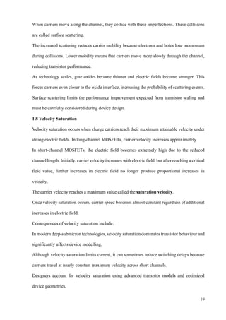
1.7 Surface Scattering
Surface scattering is a mobility degradation effect that becomes significant in short-channel
MOSFETs. Mobility refers to the ability of charge carriers (electrons or holes) to move through
the semiconductor material under the influence of an electric field.
Figure: Surface scattering in MOSFET
In MOSFET operation, applying a gate voltage creates an inversion layer near the silicon-silicon
dioxide interface. As the gate voltage increases, carriers are pulled closer to this interface.
However, the interface is not perfectly smooth. It contains:
19.
19
When carriers movealong the channel, they collide with these imperfections. These collisions
are called surface scattering.
The increased scattering reduces carrier mobility because electrons and holes lose momentum
during collisions. Lower mobility means that carriers move more slowly through the channel,
reducing transistor performance.
As technology scales, gate oxides become thinner and electric fields become stronger. This
forces carriers even closer to the oxide interface, increasing the probability of scattering events.
Surface scattering limits the performance improvement expected from transistor scaling and
must be carefully considered during device design.
1.8 Velocity Saturation
Velocity saturation occurs when charge carriers reach their maximum attainable velocity under
strong electric fields. In long-channel MOSFETs, carrier velocity increases approximately
In short-channel MOSFETs, the electric field becomes extremely high due to the reduced
channel length. Initially, carrier velocity increases with electric field, but after reaching a critical
field value, further increases in electric field no longer produce proportional increases in
velocity.
The carrier velocity reaches a maximum value called the saturation velocity.
Once velocity saturation occurs, carrier speed becomes almost constant regardless of additional
increases in electric field.
Consequences of velocity saturation include:
In modern deep-submicron technologies, velocity saturation dominates transistor behaviour and
significantly affects device modelling.
Although velocity saturation limits current, it can sometimes reduce switching delays because
carriers travel at nearly constant maximum velocity across short channels.
Designers account for velocity saturation using advanced transistor models and optimized
device geometries.
20.
20
1.9 Impact Ionization
Impactionization is a high-field effect that occurs near the drain region of short-channel
MOSFETs. As carriers travel through the channel toward the drain, they experience extremely
strong electric fields. These electric fields accelerate the carriers to very high energies.
When these energetic carriers collide with silicon atoms, they may transfer sufficient energy to
break covalent bonds within the crystal lattice. This process generates additional electron-hole
pairs.
This phenomenon is called impact ionization.
Impact ionization is particularly important because it serves as the primary mechanism
responsible for hot-carrier generation.
1.10 Hot Electron Effect
The Hot Electron Effect is one of the most serious reliability problems in short-channel
MOSFETs. It occurs when electrons gain very high kinetic energy while traveling through
regions of strong electric field, particularly near the drain.
Under normal conditions, electrons possess thermal energy corresponding to room temperature.
However, in short-channel devices, strong electric fields accelerate electrons to energies much
higher than thermal equilibrium values. These highly energetic carriers are called hot electrons.
When hot electrons reach the drain region, several undesirable events can occur:
Electron Injection into Gate Oxide
Some hot electrons gain sufficient energy to overcome the silicon-silicon dioxide energy barrier
and enter the gate oxide.
These electrons become trapped inside the oxide layer, causing:
Interface State Generation
Hot carriers can damage the silicon-oxide interface by breaking chemical bonds. This creates
interface traps that further degrade device characteristics.
21.
21
Hot electron degradationis a major reliability concern because it accumulates over time and
can eventually cause circuit failure.
22.
22
MODULE –II
LOW-POWER CIRCUITDESIGN APPROACHES
Course Outcomes
After successful completion of this module, students should be able to:
CO2 Interpret the low power circuit design approaches for different level
measures
Understand
CO3 Make use of trends in VLSI implement low power adders Embedded
hardware and software development cycles and tools.
Apply
2.1 Low-Power Design through Voltage Scaling
Voltage scaling is one of the most effective techniques used in low-power VLSI circuit design
to reduce the power consumption of integrated circuits. In CMOS circuits, dynamic power
dissipation is mainly dependent on the supply voltage, capacitance being switched, and
switching frequency. Since power consumption has a quadratic relationship with supply
voltage, reducing the operating voltage results in a significant reduction in power dissipation.
The dynamic power consumed in a CMOS circuit is expressed as proportional to
(V_{DD}^{2}), where (V_{DD}) is the supply voltage. Therefore, lowering the supply voltage
is considered a highly efficient method for reducing energy consumption in portable and
battery-operated electronic devices such as mobile phones, wearable devices, IoT systems, and
embedded processors.
However, reducing the supply voltage introduces challenges such as reduced circuit speed,
increased sensitivity to noise, and higher influence of leakage currents. When the supply voltage
is lowered, the drive capability of MOS transistors decreases because the voltage difference
between the gate and source terminals becomes smaller. This results in increased propagation
delay and slower circuit operation. To overcome these limitations, advanced voltage scaling
techniques such as Variable Threshold CMOS (VTCMOS) and Multi-Threshold CMOS
23.
23
(MTCMOS) circuits areused. These techniques reduce power consumption while maintaining
acceptable circuit performance.
VTCMOS (Variable Threshold CMOS) Circuits
Variable Threshold CMOS (VTCMOS) is a low-power circuit design technique that reduces
leakage power by dynamically controlling the threshold voltage of MOS transistors. The
threshold voltage ((V_{TH})) is the minimum gate-to-source voltage required to turn on a MOS
transistor. The leakage current in a MOS device is strongly dependent on its threshold voltage.
A lower threshold voltage provides faster switching speed but increases leakage current,
whereas a higher threshold voltage reduces leakage current but decreases the switching speed.
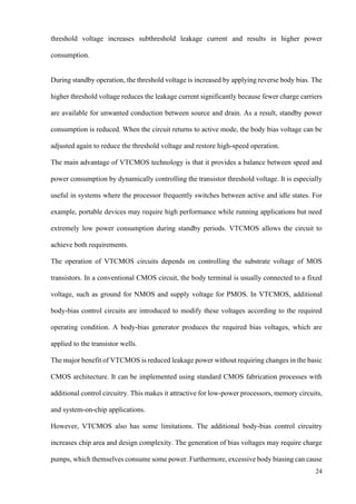
In VTCMOS circuits, the threshold voltage of the MOS transistor is adjusted by changing the
body bias voltage applied to the transistor substrate. This technique is also known as body bias
control. By applying different body voltages during different operating conditions, the circuit
can operate in high-performance mode or low-power standby mode.
Figure: Variable Threshold CMOS (VTCMOS)
During active operation, the threshold voltage is reduced by applying a suitable forward body
bias. A lower threshold voltage increases the transistor drive current, allowing faster switching
operation. This mode is useful when high performance is required. However, the reduction in
24.
24
threshold voltage increasessubthreshold leakage current and results in higher power
consumption.
During standby operation, the threshold voltage is increased by applying reverse body bias. The
higher threshold voltage reduces the leakage current significantly because fewer charge carriers
are available for unwanted conduction between source and drain. As a result, standby power
consumption is reduced. When the circuit returns to active mode, the body bias voltage can be
adjusted again to reduce the threshold voltage and restore high-speed operation.
The main advantage of VTCMOS technology is that it provides a balance between speed and
power consumption by dynamically controlling the transistor threshold voltage. It is especially
useful in systems where the processor frequently switches between active and idle states. For
example, portable devices may require high performance while running applications but need
extremely low power consumption during standby periods. VTCMOS allows the circuit to
achieve both requirements.
The operation of VTCMOS circuits depends on controlling the substrate voltage of MOS
transistors. In a conventional CMOS circuit, the body terminal is usually connected to a fixed
voltage, such as ground for NMOS and supply voltage for PMOS. In VTCMOS, additional
body-bias control circuits are introduced to modify these voltages according to the required
operating condition. A body-bias generator produces the required bias voltages, which are
applied to the transistor wells.
The major benefit of VTCMOS is reduced leakage power without requiring changes in the basic
CMOS architecture. It can be implemented using standard CMOS fabrication processes with
additional control circuitry. This makes it attractive for low-power processors, memory circuits,
and system-on-chip applications.
However, VTCMOS also has some limitations. The additional body-bias control circuitry
increases chip area and design complexity. The generation of bias voltages may require charge
pumps, which themselves consume some power. Furthermore, excessive body biasing can cause
25.
25
reliability problems dueto increased electric field effects and junction leakage. Therefore,
careful optimization is required to achieve the desired trade-off between power reduction and
performance.
2.2 MTCMOS (Multi-Threshold CMOS) Circuits
Multi-Threshold CMOS (MTCMOS) is another important low-power design technique that
reduces leakage power by using MOS transistors with different threshold voltages in the same
circuit. Unlike conventional CMOS circuits, where all transistors generally have the same
threshold voltage, MTCMOS uses a combination of low-threshold voltage transistors and high-
threshold voltage transistors.
Figure: Multi-threshold CMOS design for low power digital circuits
The basic idea behind MTCMOS technology is to use low-threshold voltage transistors in the
performance-critical paths and high-threshold voltage transistors in areas where speed is less
important. Low-threshold transistors provide high switching speed because they have higher
26.
26
drive current, whilehigh-threshold transistors reduce leakage current because they are less
prone to unwanted conduction.
In MTCMOS circuits, the logic gates are implemented using low-threshold voltage MOS
transistors to achieve high performance. These transistors allow fast charging and discharging
of load capacitances, resulting in reduced propagation delay. However, because low-threshold
devices have higher leakage currents, they are connected between virtual power lines and the
actual supply rails using high-threshold voltage sleep transistors.
The sleep transistors act as power switches that control the connection between the logic circuit
and the power supply or ground. During active operation, the sleep transistors are turned ON,
allowing normal circuit operation. The logic block receives the required supply voltage and
operates at high speed.
During standby operation, the sleep transistors are turned OFF. This disconnects the internal
logic circuit from the power supply, creating a virtual supply voltage difference. Since the high-
threshold sleep transistors have very low leakage current, the overall standby leakage power of
the circuit is greatly reduced. This technique is also known as power gating.
The main advantage of MTCMOS technology is that it achieves both high performance and low
power consumption. Low-threshold devices provide speed, while high-threshold devices
minimize leakage power. This makes MTCMOS suitable for modern VLSI systems where both
performance and energy efficiency are important.
MTCMOS circuits are widely used in low-power processors, memory systems, and portable
electronic devices. In battery-operated systems, large portions of the circuit may remain inactive
for long periods. By using MTCMOS power gating techniques, inactive circuit blocks can be
placed into sleep mode, reducing unnecessary power consumption.
The design of MTCMOS circuits involves several challenges. The insertion of sleep transistors
increases area overhead and may affect circuit timing. When a circuit returns from standby
mode to active mode, the internal nodes need to be restored to their original states, causing
27.
27
wake-up delay. Thesize of sleep transistors must be carefully selected because small sleep
transistors increase voltage drop, while large sleep transistors increase area and capacitance.
Another important consideration in MTCMOS design is the effect of power supply noise. When
multiple blocks switch between sleep and active modes simultaneously, large current variations
may occur, leading to ground bounce and supply voltage fluctuations. Proper power
management techniques are required to overcome these issues.
Comparison of VTCMOS and MTCMOS Techniques
VTCMOS and MTCMOS are both effective approaches for reducing power consumption in
CMOS circuits, but they operate using different principles. VTCMOS reduces leakage power
by dynamically adjusting the threshold voltage through body bias control, whereas MTCMOS
reduces leakage power by using multiple transistor threshold voltages and power gating
techniques.
VTCMOS provides continuous control of threshold voltage and allows smooth adjustment
between high-performance and low-power modes. It is suitable for systems requiring frequent
switching between operating conditions. MTCMOS provides stronger leakage reduction
because it can completely disconnect inactive circuits from the power supply during standby
operation.
VTCMOS requires additional body bias generation circuits, while MTCMOS requires
additional sleep transistors. VTCMOS mainly reduces leakage by controlling transistor
characteristics, whereas MTCMOS reduces leakage by controlling the power connection of
circuit blocks.
Both techniques are widely used in modern low-power VLSI design. VTCMOS is preferred
when dynamic adjustment of performance and power is required, while MTCMOS is preferred
for applications requiring extremely low standby power. In advanced semiconductor
28.
28
technologies, these techniquesare often combined with other approaches such as clock gating,
power gating, and dynamic voltage scaling to achieve highly efficient low-power systems.
2.3 Architectural Level Approach – Pipelining and Parallel Processing Approaches
In low-power VLSI circuit design, the architectural level approach focuses on reducing power
consumption by modifying the overall system organization and data processing methods rather
than optimizing only individual circuit components. At the architectural level, designers analyze
the functionality of a system and restructure the hardware architecture to achieve better
performance with reduced power dissipation. Since power consumption in VLSI systems is
strongly related to switching activity, clock frequency, operating voltage, and hardware
utilization, architectural techniques aim to reduce unnecessary operations, minimize switching
transitions, and improve computational efficiency. Two important architectural techniques used
for low-power design are pipelining and parallel processing approaches.
Figure: Processor with multiple functional units
Pipelining Approach
Pipelining is an architectural technique in which a complex operation is divided into a number
of smaller sequential stages, and each stage performs a specific part of the operation
simultaneously with other stages. The basic idea of pipelining is similar to an assembly line in
manufacturing, where different workers perform different tasks at the same time to complete
29.
29
multiple products efficiently.In VLSI systems, instead of completing an entire operation in a
single clock cycle, the operation is divided into multiple stages separated by registers. Each
stage processes a portion of the data, and the output of one stage becomes the input for the next
stage.
In a conventional non-pipelined system, a complete operation is performed by a single
processing unit, which may require a long propagation delay. The clock frequency must be
reduced to allow sufficient time for the entire operation to complete. However, in a pipelined
system, the critical path delay is divided among multiple stages. This allows the circuit to
operate at a higher clock frequency because each stage has a smaller delay. Therefore,
pipelining improves the throughput of the system, meaning more operations can be completed
in a given time.
From the low-power VLSI perspective, pipelining helps in reducing power consumption by
allowing voltage scaling. Since the delay of a circuit decreases when the critical path is divided
into smaller sections, the supply voltage can be reduced while maintaining the required
performance level. Dynamic power dissipation in CMOS circuits is proportional to the square
of the supply voltage. Therefore, reducing the operating voltage significantly decreases power
consumption. Pipelining enables this voltage reduction because the performance loss caused by
lowering the voltage can be compensated by the improved speed obtained from pipeline stages.
For example, consider a processor performing a multiplication operation. In a non-pipelined
multiplier, the complete multiplication process may require a large combinational circuit with
high delay. The circuit must operate at a high voltage to achieve the required speed. In a
pipelined multiplier, the multiplication process can be divided into several stages such as partial
product generation, addition of partial products, and final result generation. Each stage performs
a smaller task, allowing the circuit to operate efficiently at a lower voltage.
However, pipelining also introduces additional hardware in the form of pipeline registers. These
registers consume power because they require clock signals and involve charging and
30.
30
discharging of internalcapacitances. The clock distribution network associated with pipeline
registers contributes to clock power dissipation. Therefore, the design of a low-power pipeline
requires careful optimization of the number of stages, register size, and clock management
techniques.
Another important factor in pipelined circuits is clock gating. Since pipeline stages may not
always be active, clock gating can be used to disable the clock signal to inactive stages. This
reduces unnecessary switching activity and decreases dynamic power consumption. Similarly,
techniques such as operand isolation can prevent unnecessary data transitions in unused pipeline
units.
Pipelining is widely used in modern low-power processors, digital signal processors,
multimedia systems, and communication circuits. It provides a balance between performance
improvement and power reduction. By increasing throughput and enabling lower voltage
operation, pipelining becomes an important architectural technique for designing energy-
efficient VLSI systems.
Parallel Processing Approach
Parallel processing is another important architectural technique used for low-power VLSI
design. In parallel processing, multiple processing units or hardware blocks perform different
parts of a task simultaneously. Instead of increasing the speed of a single processing unit,
parallel processing improves performance by distributing the workload among multiple units.
This allows a system to complete more operations within the same time period.
The main concept behind parallel processing is to divide a large computational task into smaller
independent tasks and execute them concurrently. For example, in a digital signal processing
application, multiple data samples can be processed simultaneously using multiple arithmetic
units. Similarly, in image processing systems, different pixels or image sections can be
processed in parallel.
31.
31
In low-power circuitdesign, parallel processing provides an advantage because it allows the
operating frequency of individual processing elements to be reduced. Since power dissipation
increases with clock frequency, lowering the operating frequency reduces dynamic power
consumption. Although multiple processing units are used, the reduction in frequency and
voltage can result in overall power savings. This technique is commonly known as voltage-
frequency scaling through parallelism.
The relationship between power reduction and parallel processing can be understood by
considering a system that requires high computational speed. A traditional design may use a
single processor operating at a very high frequency and voltage to meet performance
requirements. Since dynamic power is proportional to frequency and voltage squared, the power
consumption becomes very high. Instead, the same computation can be divided among multiple
processors operating at lower frequency and voltage. The total energy required for computation
can be reduced while maintaining the same performance.
For example, suppose a processor must perform a large number of multiplication operations. A
single multiplier operating at high speed may consume significant power. Instead, multiple low-
speed multipliers can perform the operations simultaneously. Each multiplier consumes less
power due to lower voltage and frequency operation, and the total system power can be reduced.
Parallel processing is used in many modern VLSI applications such as graphics processors,
artificial intelligence accelerators, multimedia processors, and communication systems. These
applications require high computational capability while maintaining low energy consumption.
Architectures such as multi-core processors and array processors are examples of parallel
processing systems.
However, parallel processing also increases hardware complexity. More processing units
require additional area, more interconnections, and increased leakage power. As technology
scales into deep submicron regions, leakage power becomes a significant portion of total power
32.
32
consumption. Therefore, low-powerparallel architectures must carefully manage the number
of active processing units and use techniques such as power gating to switch off unused units.
Another challenge in parallel processing is data communication. Multiple processing elements
need to exchange information, and the communication network itself consumes power. Efficient
interconnection architectures and data management techniques are required to minimize
communication overhead.
Comparison of Pipelining and Parallel Processing in Low-Power Design
Pipelining and parallel processing both improve system performance, but they achieve it in
different ways. Pipelining improves performance by dividing a single operation into multiple
stages and increasing the rate at which operations are completed. Parallel processing improves
performance by executing multiple operations at the same time using multiple hardware units.
In terms of low-power design, pipelining mainly helps by reducing critical path delay and
enabling voltage scaling. Parallel processing reduces power by allowing frequency reduction
and distributing computation among multiple low-power units. Pipelining generally requires
additional registers and clock power, whereas parallel processing requires additional processing
hardware and may increase area and leakage power.
Both techniques are often combined in modern VLSI architectures to achieve high performance
with low power consumption. For example, advanced processors use multiple cores, and each
core internally uses pipelined execution units. This combination provides high computational
capability while maintaining energy efficiency.
Therefore, architectural-level approaches such as pipelining and parallel processing play a
crucial role in low-power VLSI circuit design. By optimizing the way computations are
organized and executed, these approaches reduce switching activity, enable voltage scaling,
improve performance, and contribute to the development of energy-efficient electronic systems.
2.4 Switched Capacitance Minimization Approaches
33.
33
In CMOS VLSIcircuits, dynamic power dissipation is mainly caused by the charging and
discharging of load capacitances during switching activity. This power component is
expressed as:
From the equation, it is clear that reducing the switched capacitance (Cₗ) is an effective method
for lowering power consumption. Switched capacitance minimization techniques aim to reduce
the amount of capacitance that changes voltage during circuit operation. These techniques can
be applied at different design levels: system level, circuit level, and mask/layout level.
2.5 System Level Measures
System-level measures focus on reducing power consumption by making architectural and
functional decisions before detailed circuit implementation. At this level, designers analyze the
complete system behaviour and optimize the organization of hardware blocks, data flow, and
operation scheduling to minimize unnecessary switching activity and capacitance
charging/discharging.
Since system-level decisions affect the entire chip architecture, they provide significant power
reduction compared with lower-level techniques. The main objective is to reduce the number
of active components, reduce data movement, and avoid unnecessary computations.
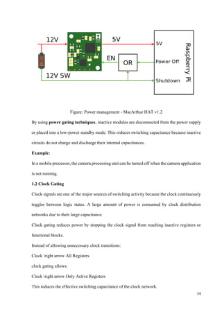
1.1 Power Management and Module Shutdown
One important system-level technique is disabling unused modules when they are not required.
Many modern VLSI systems contain multiple functional units such as processors, memory
blocks, communication modules, and peripherals. Keeping all blocks active continuously
increases switching activity and power consumption.
34.
34
Figure: Power management- MacArthur HAT v1.2
By using power gating techniques, inactive modules are disconnected from the power supply
or placed into a low-power standby mode. This reduces switching capacitance because inactive
circuits do not charge and discharge their internal capacitances.
Example:
In a mobile processor, the camera processing unit can be turned off when the camera application
is not running.
1.2 Clock Gating
Clock signals are one of the major sources of switching activity because the clock continuously
toggles between logic states. A large amount of power is consumed by clock distribution
networks due to their large capacitance.
Clock gating reduces power by stopping the clock signal from reaching inactive registers or
functional blocks.
Instead of allowing unnecessary clock transitions:
Clock right arrow All Registers
clock gating allows:
Clock right arrow Only Active Registers
This reduces the effective switching capacitance of the clock network.
35.
35
Operand Isolation
In manysystems, some inputs may change even when the output of a functional block is not
required. These input transitions cause unnecessary internal switching.
Operand isolation prevents unnecessary switching by holding the input operands constant when
a block is inactive.
Example:
A multiplier consumes significant power due to internal switching. If multiplication is not
required, the input values can be frozen to prevent internal transitions.
Benefits:
Architectural Optimization
Architecture plays an important role in minimizing switched capacitance. Designers can modify
the system architecture to reduce the amount of hardware activity required for computation.
Techniques include:
Parallel Processing
Multiple operations are performed simultaneously using separate hardware units. Although
hardware area increases, operating voltage and frequency can be reduced, leading to power
savings.
Pipelining
A large computation is divided into smaller stages. Each stage operates with reduced delay,
allowing lower voltage operation.
Resource Sharing
Multiple operations share the same hardware resource instead of using separate blocks.
Example:
A single arithmetic unit can perform addition and subtraction at different times rather than using
two separate units.
2.6 Circuit Level Measures
36.
36
Circuit-level measures involvemodifying the transistor-level implementation of logic circuits
to reduce capacitance and switching power. At this level, designers optimize transistor sizes,
logic structures, and circuit configurations.
Transistor Sizing Optimization
The size of MOS transistors directly affects capacitance. Larger transistors provide higher
driving capability but increase gate and diffusion capacitances.
If transistor sizes are unnecessarily large:
Therefore, transistor sizing is optimized to achieve a balance between speed and power.
Small transistors reduce capacitance but may increase delay. Hence, minimum transistor sizes
are used wherever performance requirements allow.
Logic Optimization
Logic optimization reduces unnecessary hardware and switching nodes by simplifying Boolean
expressions.
Gate Reordering
The order of inputs connected to logic gates affects switching activity. Proper arrangement of
signals can reduce unnecessary transitions.
For example, in a CMOS NAND gate, placing the least frequently switching input closer to the
output can reduce internal node charging and discharging.
Gate reordering helps:
Reducing Glitches
Glitches are unwanted temporary transitions caused by unequal propagation delays in logic
circuits. These unnecessary transitions consume additional dynamic power.
Methods to reduce glitches:
Reducing glitches decreases switching activity factor (α), thereby reducing power consumption.
2.5 Use of Low Power Logic Styles
Different logic families have different capacitance and switching characteristics.
37.
37
Mask-level measures areapplied during physical design and layout generation of the integrated
circuit. At this level, designers optimize the physical arrangement of transistors,
interconnections, and routing to reduce parasitic capacitance.
The capacitance in a chip is not only due to transistor gates but also due to interconnect wires.
Long wires introduce large parasitic capacitance, increasing power consumption.
Interconnect Optimization
Interconnect capacitance becomes dominant in deep submicron technologies. Reducing wire
length reduces parasitic capacitance.
Placement Optimization
Placement determines the physical location of cells on the chip.
Optimized placement keeps frequently communicating blocks closer together.
Example:
Processor → Cache Memory
should be placed close to reduce interconnect length.
Routing Optimization
Routing connects different circuit blocks through metal lines. Improper routing increases wire
capacitance and delay.
This minimizes parasitic capacitance.
Reduction of Diffusion Capacitance
Diffusion regions of MOS transistors contribute to parasitic capacitance.
Layout techniques reduce diffusion capacitance by:
38.
38
MODULE –III
LOW VOLTAGELOW POWER ADDER
Course Outcomes
After successful completion of this module, students should be able to:
CO4 Describe the pipelining approach for low power circuits Understand
3.1 Introduction
In modern VLSI (Very Large-Scale Integration) systems, power consumption has become one
of the most important design constraints along with speed, area, and reliability. The continuous
scaling of semiconductor technology has enabled the integration of millions and billions of
transistors on a single chip. However, as the transistor size decreases, the power density
increases, leading to problems such as excessive heat generation, reduced battery life, and
reliability issues. Therefore, designing circuits that operate at low voltage with minimum power
consumption has become essential, especially for portable and battery-operated applications
such as mobile devices, wearable electronics, IoT systems, and embedded processors.
An adder is one of the most fundamental arithmetic circuits used in digital systems. It performs
binary addition operations and acts as a basic building block in processors, arithmetic logic units
(ALUs), digital signal processors (DSPs), communication systems, and cryptographic
hardware. Since addition operations are frequently executed in most digital applications, the
power consumed by adders significantly affects the overall power consumption of a VLSI
system. Hence, the design of low-voltage low-power adders has gained significant importance
in advanced digital circuit design.
A low-voltage low-power adder is an arithmetic circuit designed to perform addition
operations while operating with a reduced supply voltage and consuming minimum power. The
main objective of such adders is to reduce energy consumption without greatly affecting
performance. By lowering the supply voltage, the dynamic power dissipation of the circuit can
39.
39
be reduced significantlybecause power consumption has a strong relationship with the square
of supply voltage.
The total power dissipation in an adder mainly consists of:
1. Dynamic Power Dissipation
2. Short Circuit Power Dissipation
3. Leakage Power Dissipation
Dynamic power occurs due to charging and discharging of internal capacitances during
switching operations. When the supply voltage is reduced, the charging and discharging energy
decreases, resulting in lower power consumption. Short circuit power is caused by the
temporary current flow between supply voltage and ground during transistor switching.
Leakage power occurs due to unwanted current flow through transistors even when they are not
actively switching. In deep submicron technologies, leakage power becomes a major concern.
The reduction of supply voltage is one of the most effective techniques for achieving low-power
operation. However, reducing voltage also decreases transistor drive strength, which increases
propagation delay and may affect the speed of the adder. Therefore, low-voltage adder design
requires a proper trade-off between power consumption, speed, and circuit complexity.
Low-power adders are designed using different circuit techniques and transistor-level
approaches. Some commonly used techniques include:
1. Voltage Scaling
Voltage scaling is the simplest and most effective method for reducing power consumption.
Since dynamic power is proportional to the square of supply voltage, lowering the operating
voltage results in significant power savings. However, voltage reduction increases delay
because transistors switch more slowly at lower voltages.
2. Transistor Sizing Optimization
The size of MOS transistors influences the speed and power consumption of an adder.
Increasing transistor size improves driving capability and reduces delay but increases
40.
40
capacitance and powerconsumption. Therefore, optimized transistor sizing is used to achieve a
balance between speed and power.
3. Pass Transistor Logic (PTL)
Pass transistor logic reduces the number of transistors required for implementing logic
functions. Fewer transistors reduce switching activity and capacitance, resulting in lower power
consumption and smaller chip area. However, voltage degradation problems may occur in pass
transistor circuits.
Transmission Gate Logic
Transmission gate-based adders use complementary MOS transistors to improve signal
transmission. They provide better voltage levels compared to pass transistor logic and are
suitable for low-voltage operation.
Static CMOS Logic
Static CMOS adders are widely used because of their high noise immunity and reliable
operation. They consume low static power and provide full voltage swing outputs. Optimized
CMOS structures are commonly used in low-power adder designs.
Adiabatic Logic
Adiabatic logic techniques reduce power loss by recovering some of the energy stored in circuit
capacitances. These circuits are designed to minimize energy dissipation during charging and
discharging operations.
Need for Low Voltage Low Power Adders
The requirement for low-voltage low-power adders arises due to several reasons:
• Battery-operated devices: Portable systems require circuits that consume less power
to extend battery life.
• High-density VLSI systems: Millions of arithmetic operations increase overall power
consumption.
• Thermal management: Lower power reduces heat generation and improves reliability.
41.
41
• Energy-efficient computing:Modern processors require efficient arithmetic units for
sustainable operation.
• Reduced chip size: Low-power techniques help reduce cooling requirements and
system cost.
Low-voltage adders are widely used in applications such as microprocessors, image processing
units, artificial intelligence hardware, wireless communication systems, and embedded systems.
The performance of these systems depends heavily on efficient arithmetic operations, making
adder optimization a major research area in low-power VLSI design.
Challenges in Low Voltage Low Power Adder Design
Although low-voltage operation provides power savings, it introduces several challenges:
• Increased delay: Lower voltage reduces transistor switching speed.
• Reduced noise margin: Small voltage differences make circuits more sensitive to
noise.
• Process variations: Manufacturing variations strongly affect low-voltage circuits.
• Leakage current increase: Smaller transistors introduce higher leakage power.
• Complex design requirements: Achieving high speed with low power requires
advanced circuit techniques.
3.2 Standard Adder Cells
A standard adder cell is a basic arithmetic building block used in digital VLSI circuits to
perform binary addition. Adders are among the most important components in processors,
digital signal processors, microcontrollers, and arithmetic logic units (ALUs). In VLSI design,
standard adder cells are designed as reusable library elements with optimized characteristics
such as low power consumption, high speed, small area, and reliable operation. These cells
are implemented using CMOS transistor technology and are used as fundamental units for
42.
42
constructing larger arithmeticcircuits such as ripple carry adders, carry look-ahead adders, and
multipliers.
The main function of an adder cell is to add binary input bits and generate two outputs: Sum
and Carry. The sum output represents the addition result of the input bits, while the carry output
represents the overflow generated during addition. Depending on the number of inputs and
functionality, adder cells are classified mainly into Half Adder cells and Full Adder cells.
Half Adder Cell
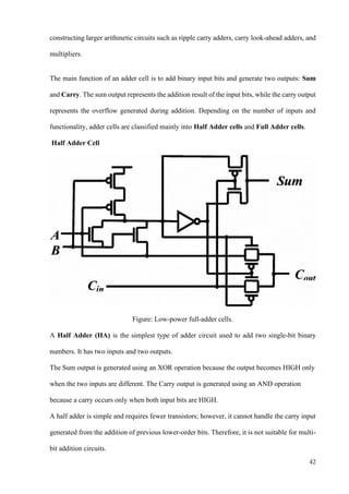
Figure: Low-power full-adder cells.
A Half Adder (HA) is the simplest type of adder circuit used to add two single-bit binary
numbers. It has two inputs and two outputs.
The Sum output is generated using an XOR operation because the output becomes HIGH only
when the two inputs are different. The Carry output is generated using an AND operation
because a carry occurs only when both input bits are HIGH.
A half adder is simple and requires fewer transistors; however, it cannot handle the carry input
generated from the addition of previous lower-order bits. Therefore, it is not suitable for multi-
bit addition circuits.
43.
43
Full Adder Cell
AFull Adder (FA) is the most commonly used standard adder cell in VLSI systems. It is
capable of adding three binary inputs: two data bits and one carry input from the previous stage.
The Boolean expressions for a full adder are:
Sum: S = A oplus B oplus Cin
Carry Output: C_{out}=AB + BC_{in}+AC_{in}
The full adder can be constructed using two half adders and one OR gate. The first half adder
adds inputs A and B, producing an intermediate sum and carry. The second half adder adds
the intermediate sum with the input carry. The two carry outputs are combined using an OR
gate to produce the final carry output.
CMOS Implementation of Standard Adder Cells
In VLSI design, adder cells are implemented using CMOS transistor structures. CMOS
technology is preferred because it provides:A conventional CMOS full adder consists of PMOS
and NMOS transistor networks. The PMOS network provides the pull-up operation, while the
NMOS network provides the pull-down operation.
The design of a CMOS adder cell focuses on optimizing:
I. Propagation Delay
a. The time required for input changes to appear at the output.
b. Lower delay improves circuit speed.
II. Power Dissipation
a. Includes switching power, leakage power, and short-circuit power.
b. Low-power adders are important for battery-operated devices.
III. Transistor Count
a. Fewer transistors reduce chip area and power consumption.
IV. Voltage Scaling Capability
44.
44
o Modern VLSIsystems operate at lower supply voltages, requiring efficient adder
designs.
Types of Standard Full Adder Cells
Conventional CMOS Full Adder
The conventional CMOS full adder uses complementary pull-up and pull-down transistor
networks.
Transmission Gate Full Adder
Transmission gate-based adders use CMOS transmission gates to reduce transistor count.
A transmission gate consists of one PMOS and one NMOS transistor connected in parallel. It
allows efficient transfer of logic signals.
Pass Transistor Full Adder
Pass transistor logic uses MOS transistors as switches to pass logic signals.
Low Power Full Adder Cells
Low-power adder cells are designed to minimize energy consumption in modern VLSI systems.
Techniques used include:
These adders are widely used in portable electronics, embedded systems, and low-power
processors.
Adder Cell Performance Parameters
Power Dissipation
Delay
Delay determines how quickly the adder produces output after receiving inputs. High-speed
applications require minimum propagation delay.
Power Delay Product (PDP)
45.
45
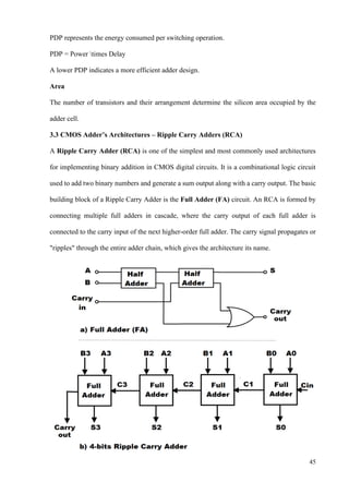
PDP represents theenergy consumed per switching operation.
PDP = Power times Delay
A lower PDP indicates a more efficient adder design.
Area
The number of transistors and their arrangement determine the silicon area occupied by the
adder cell.
3.3 CMOS Adder’s Architectures – Ripple Carry Adders (RCA)
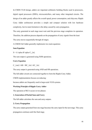
A Ripple Carry Adder (RCA) is one of the simplest and most commonly used architectures
for implementing binary addition in CMOS digital circuits. It is a combinational logic circuit
used to add two binary numbers and generate a sum output along with a carry output. The basic
building block of a Ripple Carry Adder is the Full Adder (FA) circuit. An RCA is formed by
connecting multiple full adders in cascade, where the carry output of each full adder is
connected to the carry input of the next higher-order full adder. The carry signal propagates or
"ripples" through the entire adder chain, which gives the architecture its name.
46.
46
In CMOS VLSIdesign, adders are important arithmetic building blocks used in processors,
digital signal processors (DSPs), microcontrollers, and many other integrated circuits. The
design of an adder greatly affects the overall speed, power consumption, and chip area. Ripple
Carry Adder architecture provides a simple and compact solution with low hardware
complexity, but its main limitation is the delay caused by carry propagation.
The carry generated at each stage must wait until the previous stage completes its operation.
Therefore, the addition process depends on the propagation of carry signals from the least
The carry moves sequentially through all stages.
A CMOS Full Adder generally implements two main equations:
Sum Equation
S = A oplus B oplus C_{in}
The sum output is generated using XOR operations.
Carry Equation
C_{out}=AB + BC_{in}+AC_{in}
The carry output is generated using AND and OR operations.
The full adder circuits are connected together to form the Ripple Carry Adder.
CMOS implementation focuses on reducing:
because adders are frequently used in large-scale VLSI systems.
Working Principle of Ripple Carry Adder
The operation of RCA occurs in two phases:
1. Generation of Partial Sum and Carry
The full adder calculates the sum and carry outputs.
2. Carry Propagation
The carry output generated from one stage becomes the carry input for the next stage. This carry
propagation continues until the final stage.
47.
47
The worst-case conditionoccurs when the carry generated at the first stage travels through all
stages before producing the final output.
Example:
For an 8-bit RCA:
C_0 right arrow C_1 right arrow C_2 right arrow ... right arrow C_8
The carry must pass through eight full adders before the final answer is available.
Advantages of Ripple Carry Adder
Simple Architecture
The RCA has a very simple design because it only requires cascading full adders. This makes
it easy to design and implement in CMOS circuits.
Low Hardware Complexity
Compared with advanced adder architectures, RCA requires fewer transistors and less circuit
area.
Low Power Consumption
Because of the reduced number of logic elements, RCA consumes less power compared with
complex carry acceleration techniques.
Regular Layout
The repeated structure of full adders allows easier VLSI layout design and efficient chip
implementation.
High Propagation Delay
The major drawback of RCA is carry propagation delay. Since each full adder waits for the
previous carry output, the delay increases linearly with the number of bits.
For an n-bit RCA:
Delay propto n
As the number of bits increases, speed decreases.
Poor Performance for Large Word Sizes
48.
48
Large adders suchas:
• 16-bit
• 32-bit
• 64-bit
require more time because the carry must travel through many stages.
Reduced Operating Speed
The sequential carry movement limits the maximum operating frequency of the system.
Power Dissipation in CMOS Ripple Carry Adders
In low-power VLSI design, reducing power consumption of RCA is important. Power
dissipation occurs due to:
Switching Power
When input signals change, internal capacitances charge and discharge.
P_{dynamic}= alpha C_L V_{DD}^{2} f
where:
• α = switching activity
• CL = load capacitance
• VDD = supply voltage
• f = operating frequency
Short Circuit Power
During switching, both PMOS and NMOS transistors may conduct simultaneously, creating a
direct path between supply and ground.
Leakage Power
Due to reduced CMOS transistor dimensions, leakage current increases even when circuits are
idle.
Low-power RCA designs reduce these effects by:
• Reducing transistor count
49.
49
• Using efficientCMOS logic styles
Ripple Carry Adder Delay Analysis
The delay of RCA depends mainly on carry propagation delay.
For a single full adder:
T_{FA}=T_{carry}+T_{sum}
For an n-bit RCA:
T_{RCA}= (n-1)T_{carry}+T_{sum}
where:
• (T_{carry}) = carry propagation delay
• (T_{sum}) = sum generation delay
Thus, increasing the number of bits increases delay significantly.
3.4 Low-Voltage Low Power Design Techniques
Low-voltage low-power design techniques are a set of strategies used in modern VLSI systems
to reduce overall power consumption by lowering the supply voltage and optimizing circuit
operation. Since dynamic power dissipation in CMOS circuits is proportional to the square of
the supply voltage (VDD²), even a small reduction in voltage leads to a significant decrease in
power consumption. However, reducing voltage also impacts circuit speed, noise margin, and
reliability, so these techniques are carefully designed to balance power savings with
performance requirements.
One of the most fundamental approaches is voltage scaling, where the supply voltage is reduced
either globally or selectively depending on performance needs. In static voltage scaling, a fixed
lower voltage is used to reduce power, but this may degrade speed. To overcome this, modern
systems use dynamic voltage scaling (DVS) or dynamic voltage and frequency scaling (DVFS),
where voltage and clock frequency are adjusted in real time based on workload demand. When
processing demand is low, the system runs at reduced voltage and frequency, saving power
significantly.
50.
50
Another important techniqueis VTCMOS (Variable Threshold CMOS), where the threshold
voltage of transistors is dynamically adjusted using body biasing. In low-power or standby
modes, the threshold voltage is increased to reduce leakage current, while in active mode it is
lowered to maintain performance. This technique is effective in reducing subthreshold leakage
power, which has become a major concern in deep submicron technologies.
MTCMOS (Multi-Threshold CMOS) is another widely used technique where high-threshold
transistors are used to cut off power supply to inactive circuit blocks. In this approach, “sleep
transistors” are inserted between the logic block and power supply or ground. When the circuit
is idle, these sleep transistors turn off the block, significantly reducing leakage power. When
active, they turn on and allow normal operation, making this technique highly effective for
standby power reduction.
In addition to these, multi-voltage design is also used, where different sections of a chip operate
at different supply voltages based on their performance requirements. High-speed blocks
operate at higher voltage, while non-critical blocks use lower voltage, achieving an overall
reduction in power consumption. This is often combined with level shifters to ensure proper
communication between voltage domains
3.5 Trends of Technology and Power Supply Voltage
The continuous advancement in VLSI (Very Large-Scale Integration) technology has
resulted in the fabrication of millions and billions of transistors on a single chip. As
semiconductor technology progresses from larger feature sizes to smaller technology nodes, the
major objectives are to increase speed, packing density, functionality, and energy efficiency
while reducing chip area and cost. One of the most important trends in modern VLSI design is
the reduction of power supply voltage along with transistor scaling. The reduction in supply
voltage is a key technique for achieving low-power operation because dynamic power
consumption of CMOS circuits is directly proportional to the square of the supply voltage.
Therefore, lowering the supply voltage provides a significant reduction in power dissipation.
51.
51
In the earlystages of semiconductor technology, CMOS circuits operated with higher supply
voltages such as 5 V. As technology dimensions reduced, the supply voltage gradually
decreased to 3.3 V, 2.5 V, 1.8 V, 1.2 V, and below 1 V. Modern nanoscale technologies operate
with very low supply voltages, typically around 0.8 V to 1 V, to meet the requirements of
portable and battery-operated electronic devices. This trend is driven by the need for low energy
consumption in applications such as mobile phones, wearable devices, Internet of Things (IoT),
and embedded systems.
Technology Scaling Trend
Technology scaling refers to the continuous reduction of transistor dimensions such as channel
length, gate oxide thickness, and junction depth. According to semiconductor scaling trends,
every new generation of technology reduces the transistor size, allowing more transistors to be
integrated into the same chip area. For example, VLSI technology has evolved from
micrometre-scale devices to nanometer-scale technologies such as 90 nm, 65 nm, 45 nm, 32
nm, 22 nm, 14 nm, 7 nm, and 5 nm technologies.
Scaling provides several advantages:
• Increased transistor density
• Higher operating speed
However, continuous scaling also introduces challenges such as increased leakage current,
short-channel effects, process variations, and power density problems. As transistor dimensions
become smaller, controlling power consumption becomes a major concern in VLSI design.
Relationship Between Technology Scaling and Power Supply Voltage
As transistor size decreases, the supply voltage must also be reduced to maintain reliable
operation and prevent excessive electric fields inside the transistor. A higher voltage applied to
a very small transistor can damage the device due to increased electric field intensity. Therefore,
voltage scaling accompanies technology scaling.
The dynamic power dissipation in CMOS circuits is given by:
52.
52
Pdynamic = αC V² f
where:
• α = switching activity factor
• C = load capacitance
• V = supply voltage
• f = operating frequency
From this relationship, it is clear that reducing supply voltage provides a quadratic reduction in
dynamic power. For example, reducing voltage from 5 V to 1 V can theoretically reduce
dynamic power by approximately 25 times, assuming other parameters remain constant.
Evolution of Supply Voltage
The trend of supply voltage reduction with technology advancement can be summarized as:
The reduction of supply voltage has become an essential design requirement for low-power
VLSI circuits.
Impact of Reduced Supply Voltage
Reducing supply voltage provides many benefits:
Reduction in Dynamic Power
The major advantage of voltage scaling is the reduction in switching power. Since power
depends on the square of voltage, even a small reduction in voltage results in significant energy
savings.
Improved Battery Life
Portable electronic systems depend on batteries. Low supply voltage reduces energy
consumption and increases operating time, making devices more efficient.
Lower Heat Generation
Power dissipation appears as heat in integrated circuits. Reducing supply voltage decreases heat
generation and improves system reliability.
Higher Integration Capability
53.
53
Lower voltage operationenables the integration of more functional blocks on a single chip
without exceeding power limitations.
Challenges Due to Voltage Scaling
Although supply voltage reduction provides power advantages, it introduces several problems:
Reduced Noise Margin
Lower supply voltage decreases the difference between logic HIGH and logic LOW levels,
making circuits more sensitive to noise.
Performance Degradation
The reduction in supply voltage decreases transistor drive current, which can increase circuit
delay and reduce operating speed.
Increased Leakage Power
As transistor dimensions shrink, leakage currents become significant. In modern technologies,
leakage power can become comparable to switching power.
Process Variation Effects
At nanometer scales, small variations in manufacturing parameters can significantly affect
circuit performance.
Technology Trends in Low-Power VLSI
Modern VLSI design follows several approaches to overcome power challenges:
Multi-Voltage Design
Different blocks of a chip operate at different voltage levels depending on performance
requirements. High-performance blocks use higher voltage, while less critical blocks use lower
voltage.
Voltage Islands
Large chips are divided into voltage regions where each region operates at an optimized supply
voltage.
Dynamic Voltage Scaling (DVS)
54.
54
The supply voltageand operating frequency are dynamically adjusted according to workload
requirements. During low computational demand, voltage is reduced to save power.
Adaptive Voltage Scaling (AVS)
The voltage is automatically adjusted based on process, temperature, and performance
variations.
Future Trends
Future semiconductor technologies continue toward extremely small transistor dimensions and
ultra-low voltage operation. Emerging technologies such as FinFET, Gate-All-Around (GAA)
transistors, and advanced semiconductor materials aim to maintain performance while reducing
power consumption.
The future trend of VLSI technology focuses on:
• Sub-1 V operation
• Ultra-low leakage devices
3.6 Low-Voltage Low-Power Logic Styles
Low-Voltage Low-Power (LVLP) logic styles are circuit design techniques used in VLSI
systems to reduce power consumption while maintaining acceptable performance. As the
number of transistors increases in modern integrated circuits, power dissipation has become a
major design challenge. Reducing the supply voltage is one of the most effective methods to
lower power because dynamic power consumption depends strongly on the square of the supply
voltage. Low-voltage logic styles aim to operate circuits at reduced voltage levels while
minimizing delay, leakage current, and energy consumption.
In conventional CMOS circuits, power consumption is mainly caused by charging and
discharging of load capacitances, short-circuit currents, and leakage currents. LVLP logic styles
modify transistor structures, circuit configurations, and switching techniques to achieve better
power efficiency.
Need for Low-Voltage Low-Power Logic Styles
55.
55
The continuous scalingof CMOS technology has resulted in smaller transistor dimensions and
higher transistor density. Although scaling improves speed and integration capability, it
introduces problems such as increased leakage current, reduced noise margin, and higher power
density.
The main reasons for adopting low-voltage low-power logic styles are:
• Reduction of dynamic power consumption
• Lower heat generation
Low-voltage operation reduces the energy required for each switching operation, making it
suitable for applications such as mobile processors, IoT devices, wearable electronics, and
biomedical systems.
Conventional CMOS Logic Style
CMOS (Complementary Metal Oxide Semiconductor) logic is the most widely used logic style
in digital circuits. It consists of:
• PMOS transistors forming the pull-up network
• NMOS transistors forming the pull-down network
The PMOS network connects the output to the supply voltage (VDD), while the NMOS network
connects the output to ground.
Working Principle
When the input signal is LOW:
NMOS transistor is OFF,PMOS transistor is ON,Output becomes HIGH
When the input signal is HIGH:
NMOS transistor is ON,PMOS transistor is OFF,Output becomes LOW
The dynamic power of CMOS is approximately:
P_{dynamic}= alpha C_L V_{DD}^{2}f
where:
• α = switching activity
56.
56
• Cₗ =load capacitance
• VDD = supply voltage
• f = operating frequency
Reducing VDD is therefore an effective method for power reduction.
Pass Transistor Logic (PTL)
Pass Transistor Logic is a low-power logic style in which transistors are used as switches to
pass logic signals instead of using traditional pull-up and pull-down networks.
In PTL, an NMOS or PMOS transistor transfers input signals directly to the output node.
Working Principle
An NMOS transistor passes:
• Strong logic 0
• Weak logic 1
A PMOS transistor passes:
• Strong logic 1
• Weak logic 0
Therefore, PTL circuits often require signal restoration circuits.
Transmission Gate Logic (TGL)
Transmission Gate Logic is an improved version of pass transistor logic. It uses both NMOS
and PMOS transistors connected in parallel.
A transmission gate consists of:
One NMOS transistor,One PMOS transistor
controlled by complementary signals.
Operation
When control signal is HIGH:
NMOS and PMOS turn ON,Input is transferred to output
When control signal is LOW:
57.
57
Both transistors turnOFF,Output is isolated
Dynamic Logic
Dynamic logic is a logic design technique that uses temporary charge storage on capacitances
to perform logic operations.
Unlike static CMOS, dynamic logic uses:
PMOS precharge transistor,NMOS evaluation network
Two Operating Phases
Precharge Phase
When clock signal is LOW:
PMOS transistor turns ON,Output node charges to VDD
Evaluation Phase
When clock signal is HIGH:
PMOS turns OFF,NMOS network evaluates the logic function
If the NMOS path exists, output discharges to ground.
Dynamic logic is used in high-performance processors.
Domino Logic
Domino logic is an improved form of dynamic logic that combines dynamic logic with a static
CMOS inverter.
It is called domino logic because signals propagate through multiple stages like falling
dominoes.
Structure
A domino logic gate contains:
Dynamic logic block,Inverter,Keeper transistor
The keeper transistor maintains the stored charge and reduces leakage effects.
Differential Cascode Voltage Switch Logic (DCVSL)
DCVSL is a low-power logic style that uses differential signals and complementary inputs.
58.
58
MODULE –IV
LOW-VOLTAGE LOW-POWERMULTIPLIERS
Course Outcomes
After successful completion of this module, students should be able to:
CO5 Classify different types of multipliers used to design low
power multipliers.
Understand
4.1. Introduction
Multiplication is one of the most important arithmetic operations performed in digital systems
and is widely used in processors, digital signal processing (DSP) systems, image processing
units, artificial intelligence hardware, communication systems, and embedded applications. In
VLSI circuits, multipliers are considered one of the most complex and power-consuming
arithmetic blocks because they require a large number of logic gates and interconnections to
perform high-speed computations.
The performance of a digital system is highly dependent on the efficiency of its multiplier
circuit. A good multiplier architecture should provide high speed, low power consumption,
small chip area, and reliable operation. As the demand for portable electronic devices increases,
low-power multiplier design has become an important research area in VLSI technology.
In binary multiplication, the multiplication process involves generating partial products and
adding them together to obtain the final result. The number of partial products increases with
the size of the input operands. For example, multiplying two n-bit numbers requires n partial
products, and these partial products must be added efficiently. The design of the partial product
generation and addition stages determines the overall performance of the multiplier.
Modern VLSI multiplier designs focus on reducing propagation delay, minimizing power
dissipation, and decreasing hardware complexity. Various multiplier architectures have been
developed, such as array multipliers, tree multipliers, Booth multipliers, and modified multiplier
59.
59
structures. Each architectureprovides different advantages depending on the application
requirements.
4.2. Overview of Multiplication
Multiplication is the process of adding a number to itself multiple times according to the value
of another number. In digital systems, multiplication is performed using binary numbers. A
binary multiplier multiplies two binary operands called the multiplicand and multiplier to
produce a binary product.
For two binary numbers:
A × B = Product
where:
• A → Multiplicand
• B → Multiplier
• Product → Result of multiplication
Binary multiplication follows a procedure similar to decimal multiplication. The multiplier bits
are examined one by one, and depending on whether the bit is 0 or 1, the multiplicand is either
ignored or added. The generated intermediate results are called partial products.
The multiplication operation mainly consists of two steps:
Partial Product Generation
The first step is generating partial products by performing AND operations between the bits of
the multiplicand and multiplier.
For n-bit multiplication:
• Each multiplier bit produces one partial product.
• The number of partial products is equal to the number of multiplier bits.
Partial Product Addition
The generated partial products are added using adders. The speed of the multiplier mainly
depends on the efficiency of this addition process.
60.
60
A simple multiplieruses ripple carry adders, but they introduce large delay due to carry
propagation. Advanced multiplier architectures use carry-save adders, Wallace trees, and
optimized addition techniques to improve performance.
4.3. Types of Multiplier Architectures
Different multiplier architectures are designed based on speed, area, and power requirements.
The major types of multiplier architectures are:
4.3.1. Array Multiplier
Array multiplier is one of the simplest and most commonly used multiplier architectures. It
consists of a regular arrangement of AND gates and adders.
The partial products are generated using AND gates, and the addition of partial products is
performed using half adders and full adders.
Advantages:
• Simple structure
• Easy implementation
• Regular layout suitable for VLSI fabrication
Disadvantages:
• Requires large hardware area
• Higher power consumption
• Delay increases for larger bit sizes
Array multipliers are mainly used where simple design and regular structure are more important
than speed.
4.3.2. Tree Multiplier
Tree multipliers reduce the addition delay by arranging partial product addition in a tree
structure.
61.
61
Instead of addingpartial products sequentially, tree structures add multiple partial products
simultaneously.
Tree multipliers are commonly used in high-performance processors and DSP applications.
4.3.3. Braun Multiplier
Braun multiplier is a type of parallel array multiplier used for unsigned binary multiplication.
4.3.4. Baugh-Wooley Multiplier
Baugh-Wooley multiplier is designed specifically for signed binary multiplication using two's
complement representation.
Figure: 4 bits Baugh Wooley multiplier.
4.3.5. Booth Multiplier
Booth multiplier is an efficient multiplier architecture that reduces the number of partial
products by encoding the multiplier bits.
4.4. Braun Multiplier
62.
62
The Braun multiplieris a parallel multiplier architecture used for unsigned binary
multiplication. It is also known as a carry-save array multiplier because it uses carry-save
addition techniques.
A Braun multiplier consists of:
AND gates for partial product generation, Full adders for partial product accumulation,
Carry propagation adders for final addition
Figure: 4×4 bit basic Braun multiplier
For an n-bit Braun multiplier:
n × n AND gates are required, Several full adders are arranged in an array structure
The multiplier generates partial products by multiplying every bit of the multiplicand with every
bit of the multiplier.
These partial products are added using full adders.
Working Principle
1. The input bits are applied to AND gates.
63.
63
2. Each ANDgate produces a partial product.
3. Full adders add the partial products.
4. The final output is obtained after carry propagation.
The Braun multiplier is suitable for applications where simplicity and regular layout are
preferred.
4.5. Baugh-Wooley Multiplier
The Baugh-Wooley multiplier is a multiplier architecture used for signed binary multiplication.
It efficiently handles two's complement numbers.
In conventional multiplication of signed numbers, sign extension creates additional complexity.
The Baugh-Wooley algorithm modifies the partial products so that signed multiplication can be
performed using the same hardware structure as unsigned multiplication.
The architecture uses AND gates, Full adders, Modified partial product generation
Need for Baugh-Wooley Multiplier
In signed multiplication:
Negative numbers are represented using two's complement. Direct multiplication creates
unwanted sign bits. Additional correction terms are required.
The Baugh-Wooley method rearranges these correction terms and integrates them into the
multiplier structure.
Working Principle
For two signed n-bit numbers:
1. Partial products are generated.
2. The sign bit multiplication is modified.
3. Complemented partial products are added.
4. Correction bits are added to obtain the final signed product.
4.6. Booth Multiplier
64.
64
Booth multiplier isan efficient multiplication technique developed by Andrew Donald Booth.
It is mainly used for signed binary multiplication and reduces the number of partial products
generated during multiplication.
The main idea of Booth multiplication is to examine consecutive bits of the multiplier and
encode multiple bits together. This reduces the number of addition operations.
In conventional multiplication:
• Every 1 in the multiplier generates a partial product.
In Booth multiplication:
Groups of bits are analyzed. Consecutive 1s are replaced by subtraction and addition operations.
Example:
A multiplier sequence:011110 can be represented as: 100000 - 000010
This reduces the number of partial products.
Booth Algorithm Steps
1. Initialize:
o Accumulator register
o Multiplier register
o Multiplicand register
2. Examine the least significant bit of multiplier and an additional previous bit.
3. According to bit patterns:
4. Perform arithmetic right shift.
5. Repeat until all bits are processed.
65.
65
MODULE –V
LOW-VOLTAGE LOW-POWERMEMORIES
Course Outcomes
After successful completion of this module, students should be able to:
CO6 Demonstrate the basic concepts of memories for designing of low
power SRAM and DRAM memories.
Apply
Introduction to Low-Voltage Low-Power Memories
Memory is one of the most important components in modern VLSI systems because it stores
and provides data required for processing operations. In advanced electronic systems such
as mobile phones, wearable devices, Internet of Things (IoT) devices, biomedical systems,
and portable computing devices, reducing power consumption has become a major design
requirement. Since memories occupy a large portion of the chip area and contribute
significantly to total power dissipation, designing low-voltage low-power memories is
essential.
Low-voltage memory design focuses on reducing the supply voltage required for memory
operation, while low-power memory design aims to minimize energy consumption during
read, write, and standby modes. Lowering the supply voltage reduces dynamic power
consumption because power is proportional to the square of supply voltage. However,
reducing voltage introduces challenges such as reduced noise margin, slower operation, and
increased sensitivity to process variations. Therefore, special circuit techniques are
developed to achieve reliable memory operation at low voltage levels.
Low-power memories are mainly designed by optimizing:
Memory cell structure, Supply voltage, Transistor sizing, Leakage current reduction,
Read/write operation circuits
Refresh mechanisms
66.
66
I. Power managementtechniques
The major types of memories used in low-power VLSI systems are:
• ROM (Read Only Memory)
• SRAM (Static Random Access Memory)
• DRAM (Dynamic Random Access Memory)
The major types of memories used in low-power VLSI systems are:
• ROM (Read Only Memory)
• SRAM (Static Random Access Memory)
• DRAM (Dynamic Random Access Memory)
5.1 Basics of ROM (Read Only Memory)
Read Only Memory (ROM) is a non-volatile memory used to permanently store data. The
stored information remains even when the power supply is removed. ROM is mainly used
for storing firmware, boot programs, lookup tables, and fixed data in digital systems.
Figure: Read Only Memory
67.
67
A ROM consistsof an array of memory cells arranged in rows and columns. The rows are
connected through word lines, and columns are connected through bit lines. The presence
or absence of a transistor connection at the intersection of word and bit lines represents
binary information.
In a ROM operation:
• A specific address activates a word line.
• The corresponding memory cells provide data through bit lines.
• Sense amplifiers detect and amplify the stored information.
ROM consumes very low standby power because no continuous data refreshing is required.
However, the programming process is usually fixed, making it less flexible compared to
other memory types.
Types of ROM:
I. Mask ROM
a. Data is programmed during manufacturing.
b. Provides high density and low cost for large-volume production.
c. Cannot be reprogrammed.
II. PROM (Programmable ROM)
a. Programmed only once by the user.
b. Uses programmable links or fuses.
III. EPROM (Erasable Programmable ROM)
a. Data can be erased using ultraviolet light.
b. Can be reprogrammed multiple times.
IV. EEPROM (Electrically Erasable Programmable ROM)
a. Data can be electrically erased and rewritten.
o Used in modern embedded systems.
5.2 Low-Power ROM Technology
68.
68
Low-power ROM technologyfocuses on reducing energy consumption during storage and data
access operations. Since ROM is mostly used in embedded systems, reducing its power
consumption improves battery life and system efficiency.
Techniques used in Low-Power ROM:
Reduced Supply Voltage
Lowering the operating voltage reduces dynamic power dissipation. Since switching power
depends on supply voltage, operating ROM at a lower voltage reduces energy consumption.
Advantages:
Less power consumption,Lower heat generation, Suitable for portable devices
Limitation:
Reduced voltage decreases noise margin and may affect reliability.
Low-Leakage Transistor Design
In nanoscale technologies, leakage current becomes a major source of power loss. Low-power
ROM uses: High threshold voltage transistors, Power gating techniques, Leakage reduction
circuits.These methods reduce standby power consumption.
Efficient Decoder Design
Memory decoders activate selected memory locations. Traditional decoders consume
significant power due to switching activity.
Low-power decoder techniques include:
Hierarchical decoding Reduced switching activity,Clock gating
These methods reduce unnecessary power dissipation.
Low-Power Sense Amplifiers
Sense amplifiers detect small voltage differences from memory cells. Low-power sense
amplifiers reduce the current required during read operations.
Improved memory efficiency
Basics of SRAM (Static Random Access Memory)
69.
69
Static Random AccessMemory (SRAM) is a volatile memory that stores data as long as power
is supplied. SRAM does not require refreshing, which makes it faster than DRAM.
SRAM most commonly refers to Static Random-Access Memory, a type of ultra-fast, volatile
computer memory used in CPU caches. Alternatively, in the cycling world, SRAM is a premier
manufacturer of high-performance bicycle components like drivetrains and brakes. It uses
latching circuitry (flip-flops) with 4 to 6 transistors to store each bit of data. It is significantly
faster and has lower latency than standard system memory (DRAM).
Figure: 6-T SRAM cell
Unlike DRAM, SRAM does not need to be constantly "refreshed" with electrical charges to
retain its data. It forms the high-speed L1, L2, and L3 cache memory found inside your
computer's CPU. It is volatile memory; once the power is disconnected, all data is lost.
Precharge and Equalization Circuit
The precharge and equalization circuit is an essential component of Static Random Access
Memory (SRAM), particularly in high-speed memory architectures. It is mainly associated with
70.
70
the bit linesthat connect the memory cells to the sense amplifiers. Before every read operation,
the bit lines must be prepared to a known voltage level so that even a very small voltage
difference created by the selected memory cell can be detected accurately. This preparation
process is called precharging. Typically, both bit lines, namely BL and BL
̅ , are charged to the
supply voltage (VDD) or sometimes to an intermediate voltage depending on the SRAM
architecture. Along with precharging, an equalization transistor connects the two bit lines
together momentarily, ensuring that both lines have exactly the same voltage before the memory
access begins. This process eliminates any residual voltage difference caused by the previous
read or write operation, thereby preventing incorrect data sensing.
When a read operation starts, the precharge transistors are turned off and the selected memory
cell is connected to the bit lines through the access transistors. Since both bit lines initially have
equal voltages, the memory cell causes only a slight voltage drop on one of the bit lines
depending on whether it stores a logic '0' or logic '1'. The sense amplifier then amplifies this
tiny voltage difference into a full digital signal. Without proper precharging and equalization,
the sense amplifier could produce incorrect outputs or require more time to determine the stored
value, thereby reducing memory speed and reliability.
From a power consumption perspective, the precharge and equalization circuit must be carefully
designed because charging and discharging the large bit-line capacitances consume
considerable dynamic power. Low-power SRAM designs reduce unnecessary precharge
operations, optimize transistor sizes, lower supply voltage, and employ conditional precharging
techniques to minimize switching activity. Thus, the precharge and equalization circuit not only
enables fast and reliable memory access but also plays a significant role in reducing power
consumption and improving the overall efficiency of modern SRAM systems used in
processors, cache memories, and embedded applications.
Low-Power SRAM Technologies
71.
71
Static Random AccessMemory (SRAM) is one of the fastest semiconductor memories and is
widely used as cache memory in processors, microcontrollers, and System-on-Chip (SoC)
devices. However, as integrated circuits become increasingly dense and portable electronic
devices demand longer battery life, reducing SRAM power consumption has become a major
research focus. Low-power SRAM technologies aim to minimize both dynamic and static
power while maintaining high speed, stability, and reliability.
Dynamic power in SRAM mainly results from charging and discharging the bit lines, word
lines, and internal node capacitances during read and write operations. This power can be
reduced by lowering the supply voltage, minimizing switching activity, shortening bit-line
lengths, and using segmented memory arrays. Techniques such as divided word lines and
hierarchical bit lines reduce the effective capacitance that must be charged during memory
access, thereby lowering dynamic power consumption. Conditional precharge techniques
further reduce unnecessary charging of bit lines, saving additional energy.
Static or leakage power has become a dominant concern in modern deep-submicron
technologies because millions of SRAM cells remain idle for long periods while continuously
consuming leakage current. To reduce leakage power, designers employ techniques such as
Multi-Threshold CMOS (MTCMOS), Variable Threshold CMOS (VTCMOS), transistor
stacking, power gating, and body biasing. High-threshold transistors are used in standby mode
to reduce leakage current, while low-threshold devices provide high-speed operation during
active mode. Power gating disconnects unused memory blocks from the power supply,
significantly reducing standby power.
Modern SRAM architectures also include assist circuits that improve read and write operations
at reduced supply voltages. Read assist techniques prevent accidental flipping of stored data,
while write assist techniques make it easier to overwrite existing data using lower voltage levels.
Emerging technologies such as FinFET SRAM, Carbon Nanotube FET SRAM, and Near-
Threshold SRAM further improve power efficiency while maintaining acceptable performance.
72.
72
Overall, low-power SRAMtechnologies combine circuit-level, architectural-level, and device-
level optimization techniques to achieve lower energy consumption without sacrificing speed
or reliability. These technologies are essential for smartphones, wearable devices, Internet of
Things (IoT) systems, embedded processors, and battery-powered electronics where energy
efficiency is a critical design requirement.
Basics of DRAM
Dynamic Random Access Memory (DRAM) is the most widely used main memory technology
in computers, servers, mobile devices, and embedded systems because it provides high storage
density at a relatively low manufacturing cost. Unlike Static Random Access Memory (SRAM),
which stores data using six transistors per memory cell, DRAM stores each bit using only one
transistor and one capacitor. This simple structure allows millions or even billions of memory
cells to be integrated onto a single chip, making DRAM much more compact and economical
for large-capacity memory applications.
In a DRAM cell, the capacitor acts as the storage element by holding an electrical charge. A
fully charged capacitor represents a binary '1', while a discharged capacitor represents a binary
'0'. The transistor functions as an access switch controlled by the word line. During a write
operation, the transistor connects the capacitor to the bit line, allowing it to either charge or
discharge depending on the input data. During a read operation, the stored charge slightly
changes the voltage on the bit line. Since this voltage difference is extremely small, a sense
amplifier detects and amplifies it into a full logic level.
One important characteristic of DRAM is that the capacitor gradually loses its stored charge
due to leakage current. Consequently, the stored information disappears after a short period
unless it is periodically refreshed. This requirement distinguishes DRAM from SRAM, which
retains data as long as power is supplied. Refresh operations are automatically performed by
the memory controller at regular intervals to restore the charge in every memory cell.
73.
73
Although refresh operationsconsume additional power and slightly reduce performance,
DRAM remains the preferred choice for primary memory because of its high storage density,
lower cost per bit, and scalability. Modern DRAM technologies include SDRAM, DDR, DDR2,
DDR3, DDR4, DDR5, and LPDDR memories, each offering higher speed, lower power
consumption, and increased bandwidth. Thus, DRAM forms the backbone of contemporary
computing systems by providing large-capacity, high-performance memory for operating
systems, applications, and data processing tasks.
Self-Refresh Circuit
A self-refresh circuit is an important power-saving feature incorporated into modern Dynamic
Random Access Memory (DRAM) devices. Since DRAM stores data as electrical charge in
tiny capacitors, the stored charge gradually leaks away over time due to leakage currents. If the
charge is not restored periodically, the stored information will be lost. Therefore, every DRAM
memory requires continuous refresh operations to maintain data integrity. Normally, these
refresh operations are controlled by the external memory controller. However, during low-
power or standby modes, continuously operating the memory controller would unnecessarily
consume power. To overcome this limitation, DRAM incorporates an internal self-refresh
circuit.
When the system enters sleep or standby mode, the self-refresh circuit takes over the
responsibility of refreshing the memory cells without requiring commands from the external
processor. An internal oscillator generates timing signals that periodically activate the refresh
circuitry. A refresh counter automatically selects each memory row sequentially, and the sense
amplifiers restore the charge stored in the capacitors. Since only the essential refresh circuitry
remains active while most other DRAM components are powered down, overall power
consumption is significantly reduced.
74.
74
The self-refresh circuitis especially important in battery-powered devices such as laptops,
smartphones, tablets, wearable electronics, and Internet of Things (IoT) systems, where
maintaining stored data while minimizing energy consumption is essential. Advanced DRAM
devices further improve self-refresh efficiency by incorporating temperature-compensated self-
refresh mechanisms. At lower temperatures, capacitor leakage is reduced, allowing refresh
operations to occur less frequently, thereby saving additional power. Conversely, at higher
temperatures, the refresh rate is automatically increased to ensure reliable data retention.
Although self-refresh consumes some energy, it requires much less power than keeping the
entire memory subsystem active. As semiconductor technology continues to scale, leakage
currents increase, making efficient self-refresh circuits even more critical. Modern low-power
DRAM standards such as LPDDR4 and LPDDR5 include highly optimized self-refresh
mechanisms that extend battery life while preserving stored information. Consequently, the
self-refresh circuit has become an indispensable component of energy-efficient memory
systems in modern electronic devices.