Fabrication of FLOTOX
(EEPROM Cell)
Sudhanshu Janwadkar, Teaching Asst, SVNIT, Surat
Lecture PPT: 24th Oct 2017
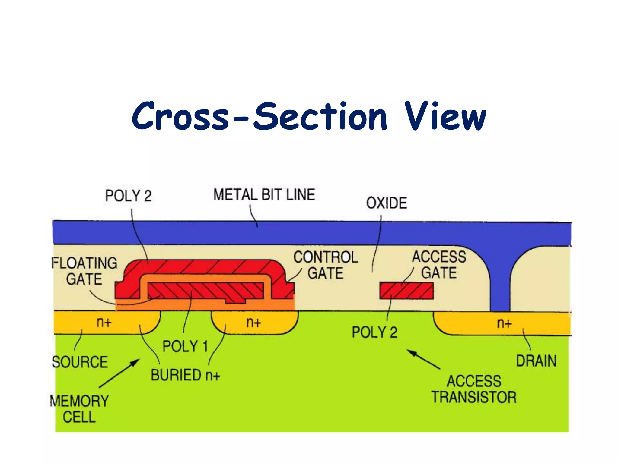
Cross-Section View
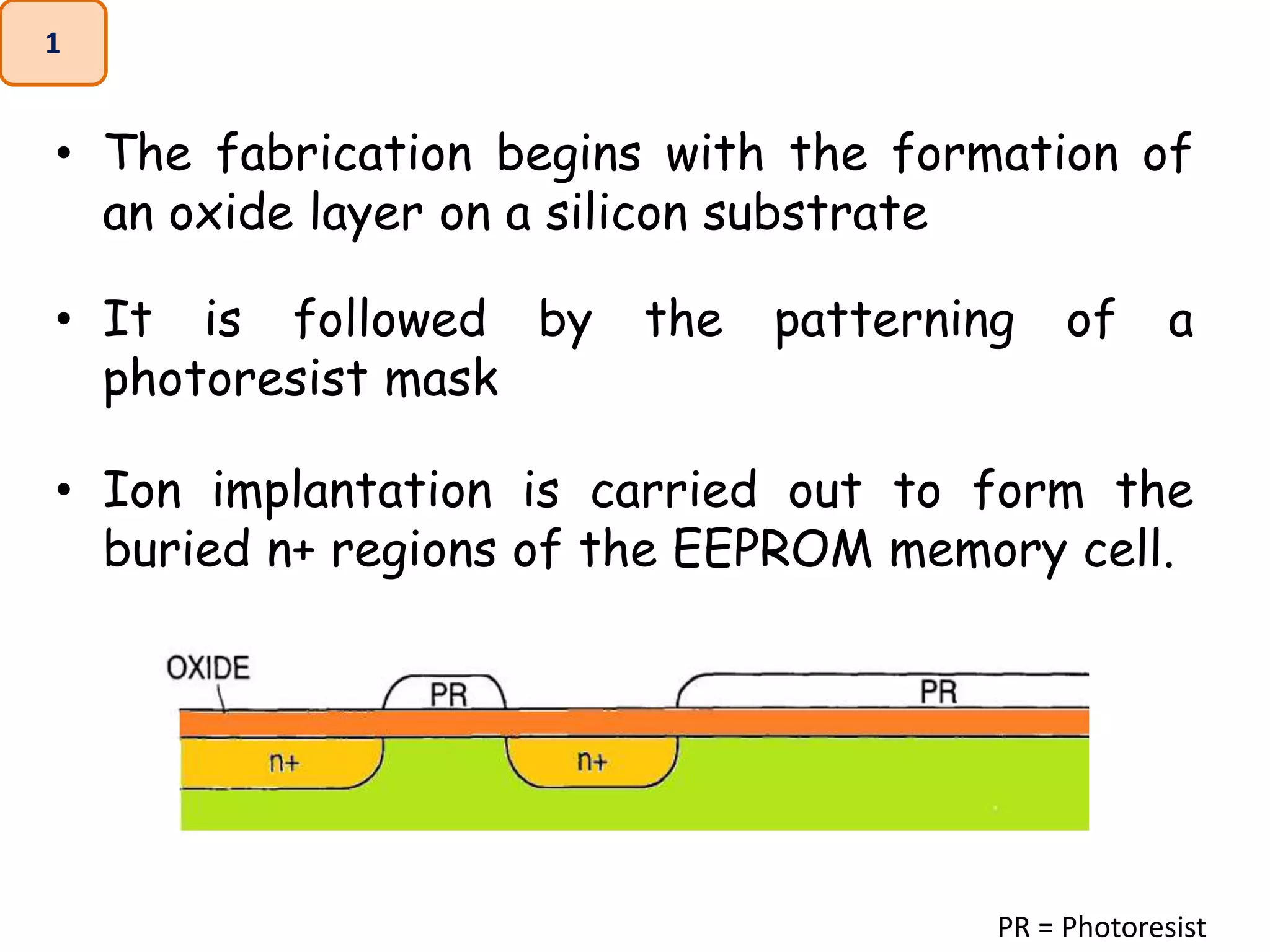
• The fabrication begins with the formation of
an oxide layer on a silicon substrate
• It is followed by the patterning of a
photoresist mask
• Ion implantation is carried out to form the
buried n+ regions of the EEPROM memory cell.
1
PR = Photoresist
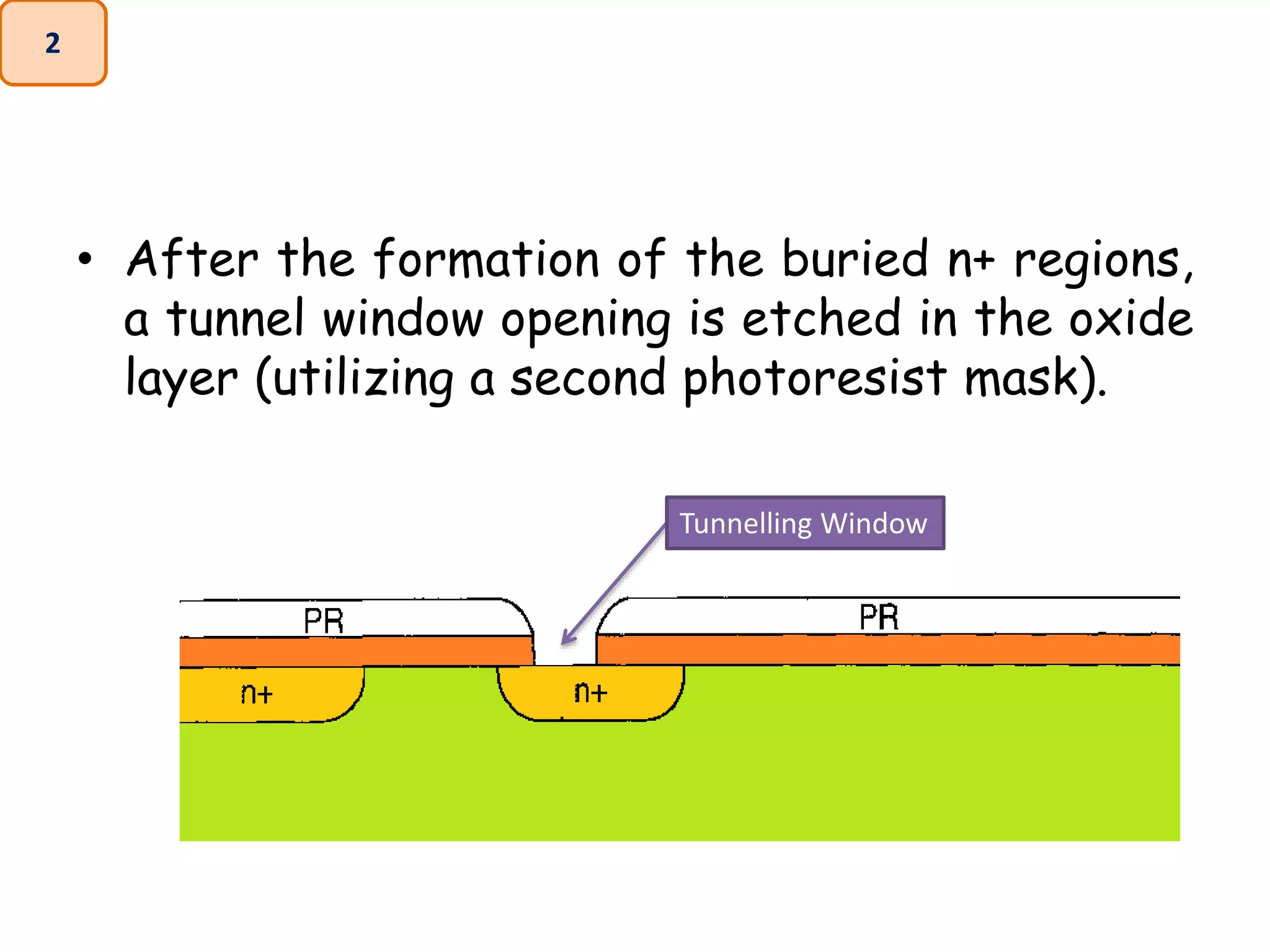
• After the formation of the buried n+ regions,
a tunnel window opening is etched in the oxide
layer (utilizing a second photoresist mask).
2
Tunnelling Window
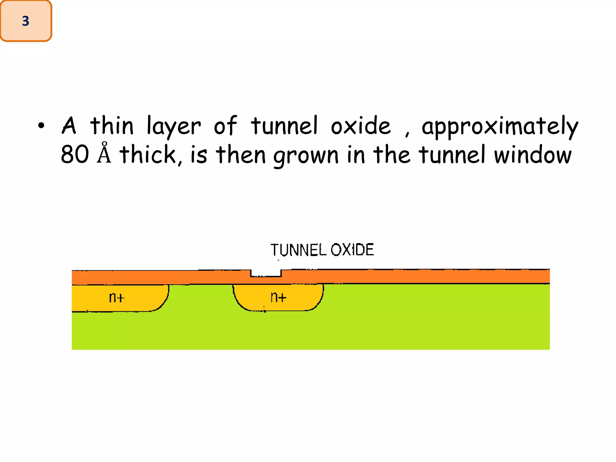
• A thin layer of tunnel oxide , approximately
80 Å thick, is then grown in the tunnel window
3
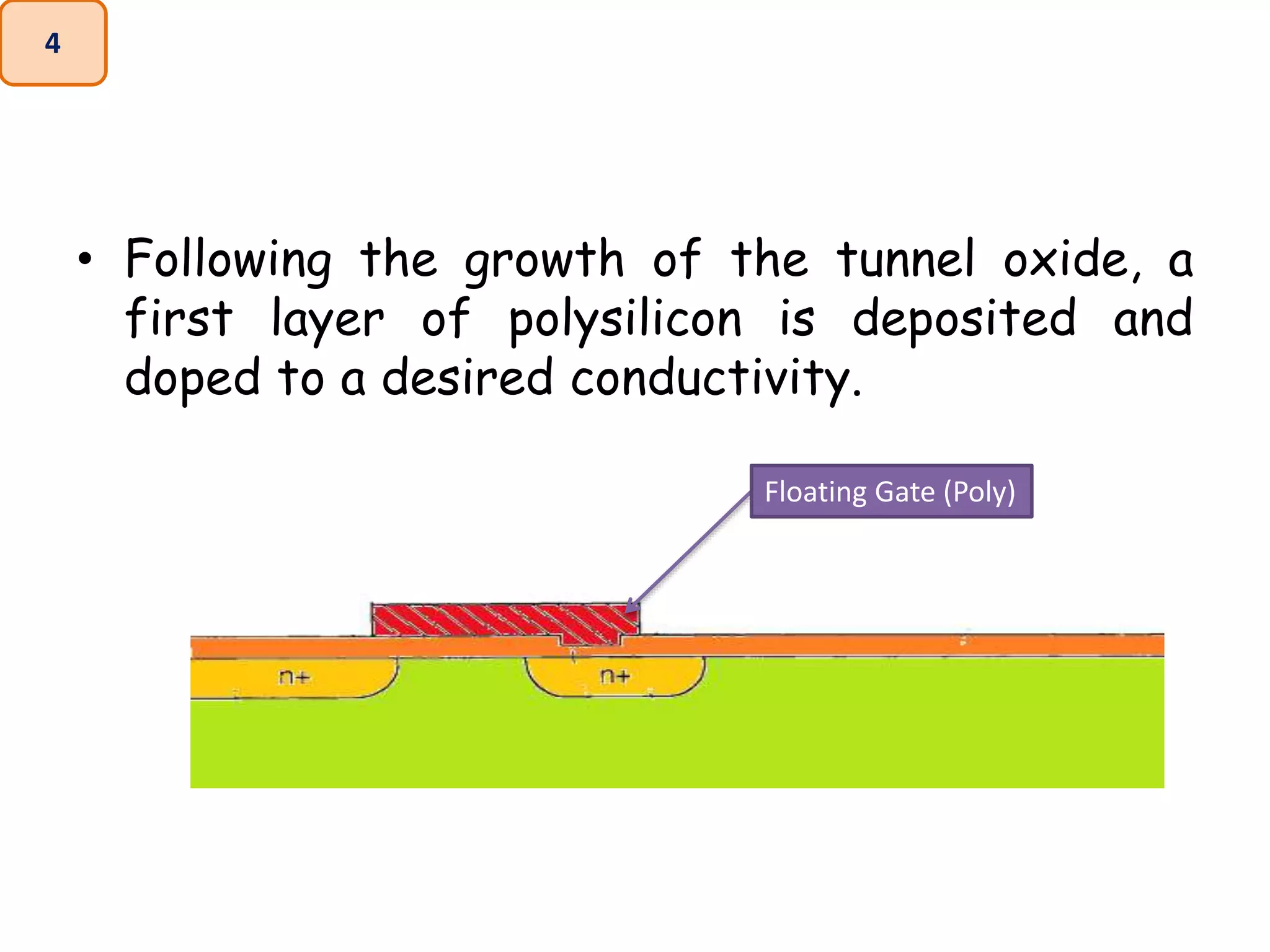
• Following the growth of the tunnel oxide, a
first layer of polysilicon is deposited and
doped to a desired conductivity.
4
Floating Gate (Poly)
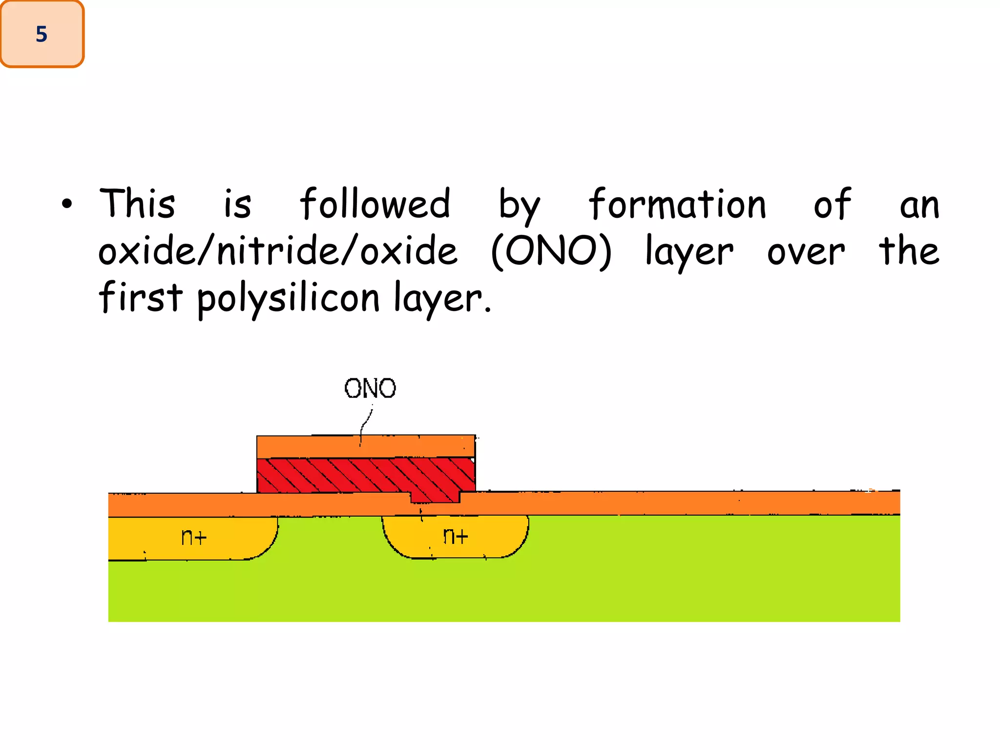
• This is followed by formation of an
oxide/nitride/oxide (ONO) layer over the
first polysilicon layer.
5
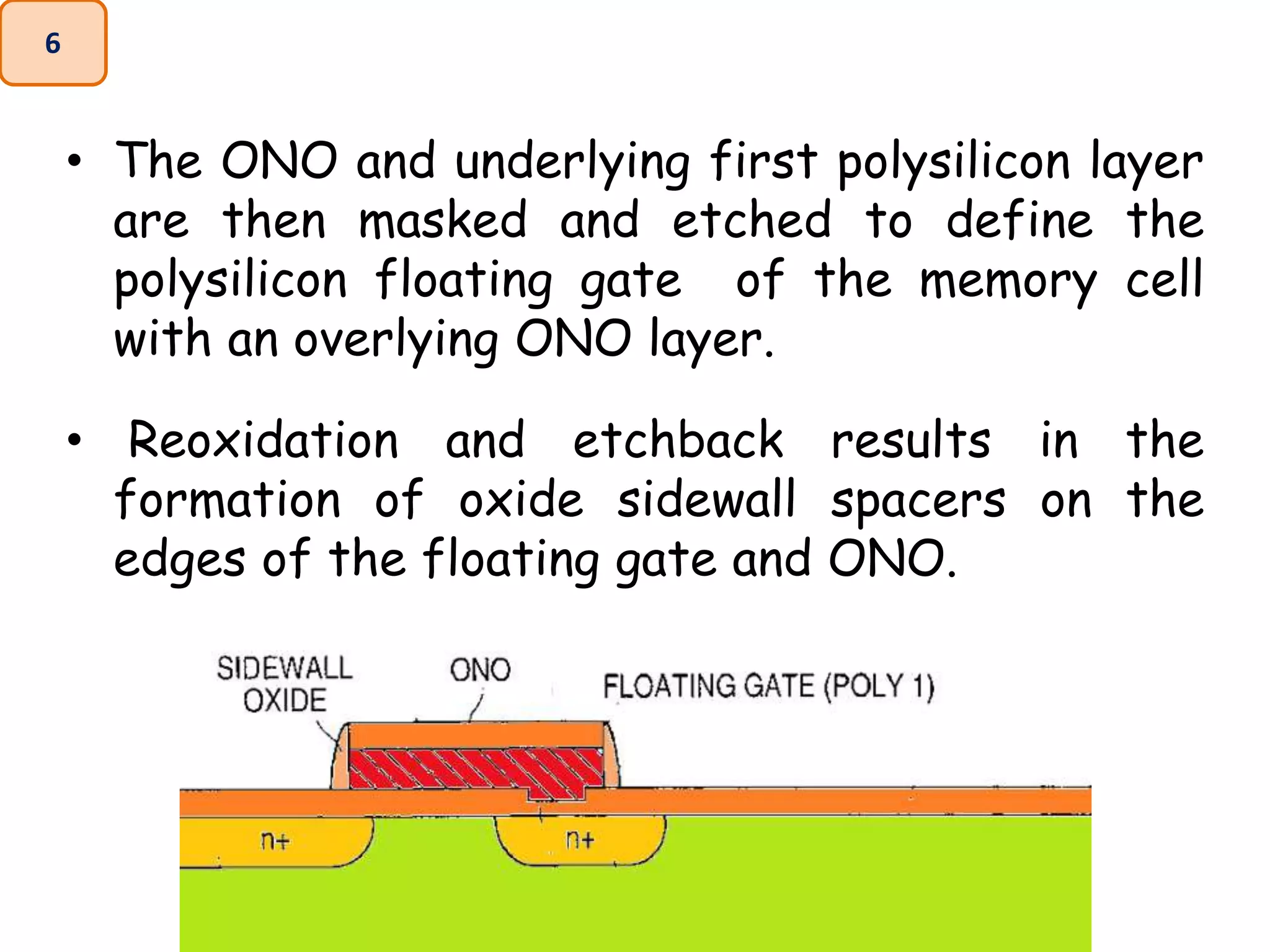
• The ONO and underlying first polysilicon layer
are then masked and etched to define the
polysilicon floating gate of the memory cell
with an overlying ONO layer.
• Reoxidation and etchback results in the
formation of oxide sidewall spacers on the
edges of the floating gate and ONO.
6
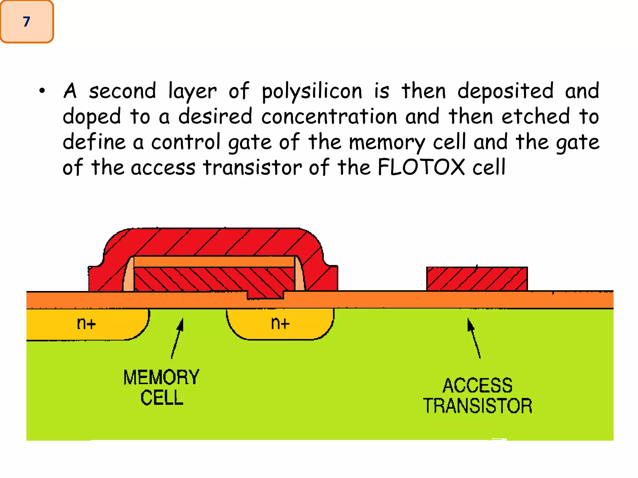
• A second layer of polysilicon is then deposited and
doped to a desired concentration and then etched to
define a control gate of the memory cell and the gate
of the access transistor of the FLOTOX cell
7
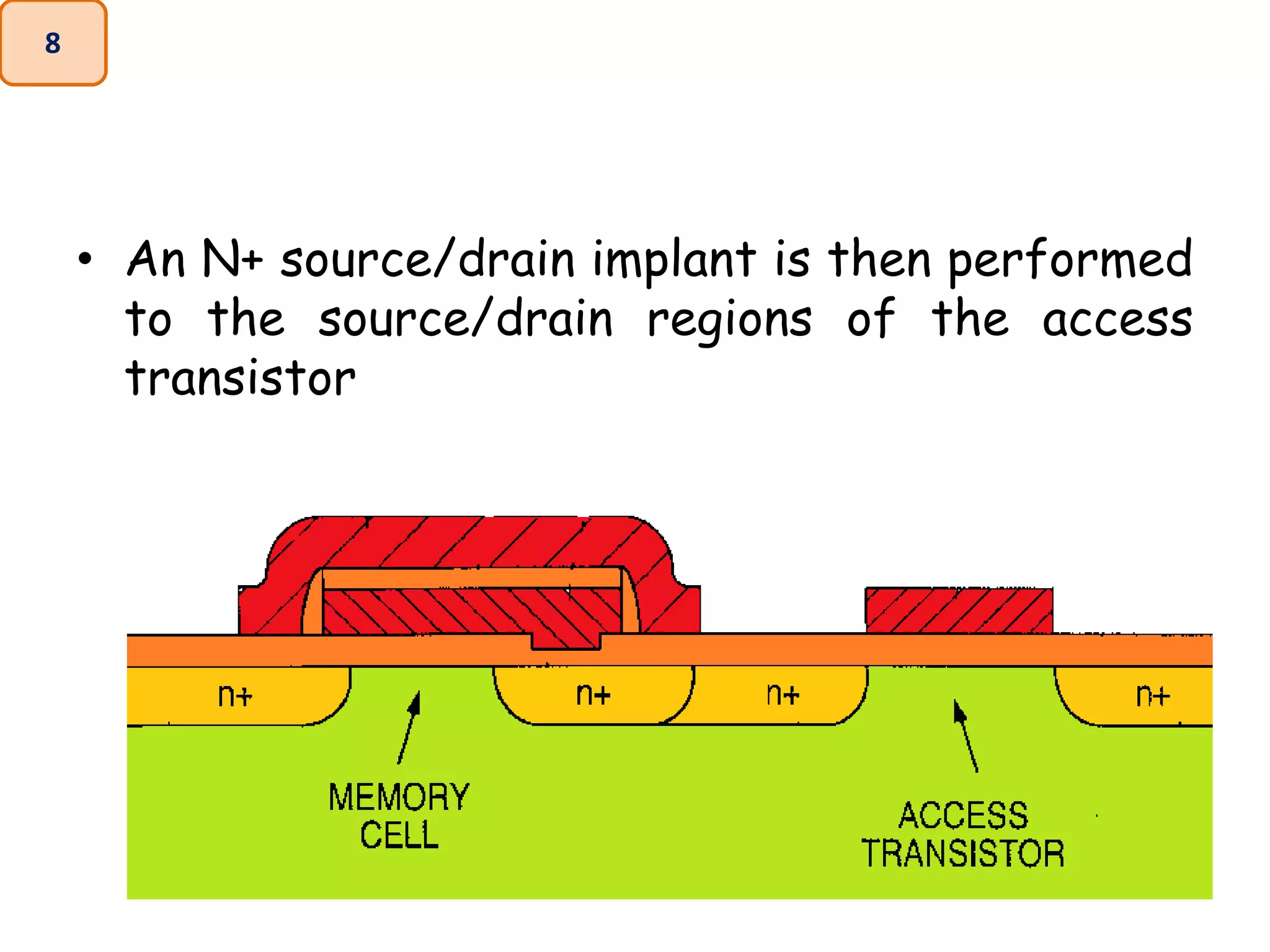
• An N+ source/drain implant is then performed
to the source/drain regions of the access
transistor
8
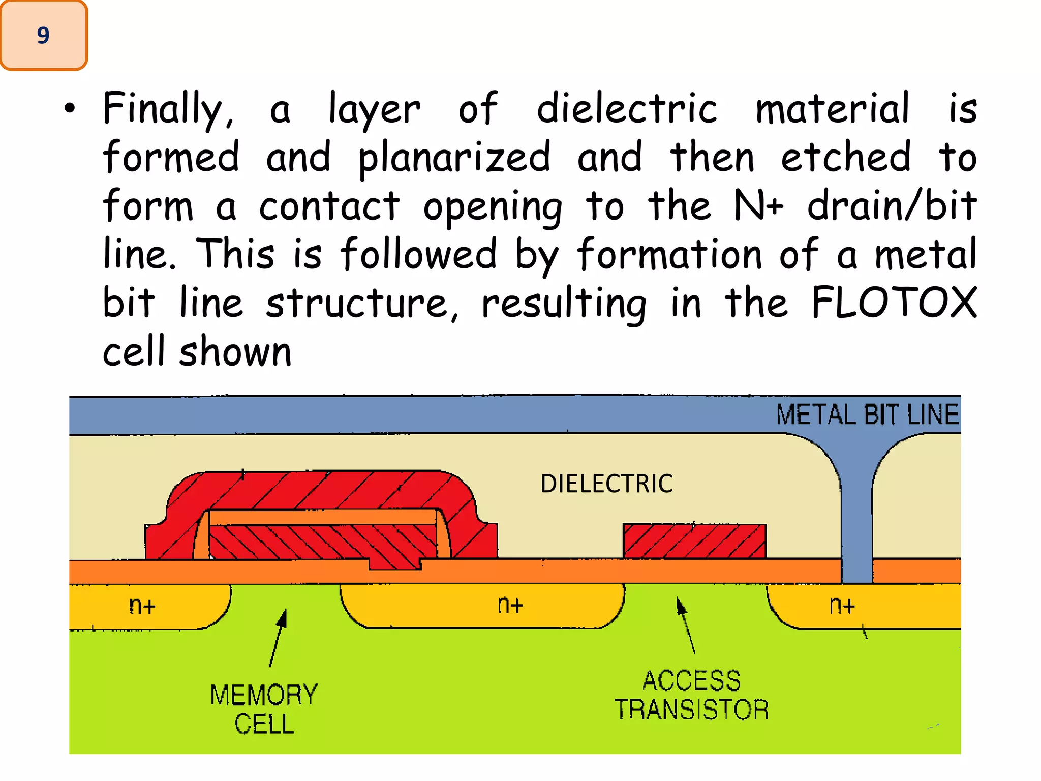
• Finally, a layer of dielectric material is
formed and planarized and then etched to
form a contact opening to the N+ drain/bit
line. This is followed by formation of a metal
bit line structure, resulting in the FLOTOX
cell shown
9
DIELECTRIC
References
• Patent US 5856222 A

Fabrication of Floating Gate MOS (FLOTOX)

  • 1.
    Fabrication of FLOTOX (EEPROMCell) Sudhanshu Janwadkar, Teaching Asst, SVNIT, Surat Lecture PPT: 24th Oct 2017
  • 2.
  • 3.
    • The fabricationbegins with the formation of an oxide layer on a silicon substrate • It is followed by the patterning of a photoresist mask • Ion implantation is carried out to form the buried n+ regions of the EEPROM memory cell. 1 PR = Photoresist
  • 4.
    • After theformation of the buried n+ regions, a tunnel window opening is etched in the oxide layer (utilizing a second photoresist mask). 2 Tunnelling Window
  • 5.
    • A thinlayer of tunnel oxide , approximately 80 Å thick, is then grown in the tunnel window 3
  • 6.
    • Following thegrowth of the tunnel oxide, a first layer of polysilicon is deposited and doped to a desired conductivity. 4 Floating Gate (Poly)
  • 7.
    • This isfollowed by formation of an oxide/nitride/oxide (ONO) layer over the first polysilicon layer. 5
  • 8.
    • The ONOand underlying first polysilicon layer are then masked and etched to define the polysilicon floating gate of the memory cell with an overlying ONO layer. • Reoxidation and etchback results in the formation of oxide sidewall spacers on the edges of the floating gate and ONO. 6
  • 9.
    • A secondlayer of polysilicon is then deposited and doped to a desired concentration and then etched to define a control gate of the memory cell and the gate of the access transistor of the FLOTOX cell 7
  • 10.
    • An N+source/drain implant is then performed to the source/drain regions of the access transistor 8
  • 11.
    • Finally, alayer of dielectric material is formed and planarized and then etched to form a contact opening to the N+ drain/bit line. This is followed by formation of a metal bit line structure, resulting in the FLOTOX cell shown 9 DIELECTRIC
  • 12.