
Recommended
Recommended
More Related Content
What's hot
What's hot (20)
Viewers also liked
Viewers also liked (13)
Similar to How to design a noise-optimized transimpedance amplifier (photodetector, photodiode) amplifier)
Similar to How to design a noise-optimized transimpedance amplifier (photodetector, photodiode) amplifier) (20)
Recently uploaded
Recently uploaded (20)
How to design a noise-optimized transimpedance amplifier (photodetector, photodiode) amplifier)
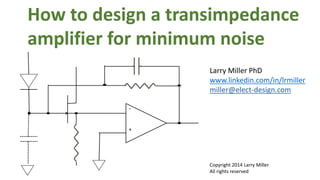
- 1. - + How to design a transimpedance amplifier for minimum noise Larry Miller PhD www.linkedin.com/in/lrmiller miller@elect-design.com Copyright 2014 Larry Miller All rights reserved
- 2. How to design a transimpedance amplifier for minimum noise Transimpedance amplifiers are used to amplify small signals from devices such as photodiodes with high source impedance. Below 1000 MHz, silicon JFET’s (junction field-effect transistors) and silicon bipolar transistors are commonly used as the first stage, because of their relatively low voltage noise. Often, integrated circuit op amps (operational amplifiers) using these transistors as first stage are used. Choosing between a JFET-input and a bipolar-transistor-input op amp is a balancing act: JFET’s typically have voltage noise spectral density of 5 nV / 𝐻𝑧 , versus the typical 5 nV / 𝐻𝑧 of bipolar transistors. Although bipolar’s have lower voltage noise than JFET’s, JFET’s have far less current noise: typically a few femtoamps / 𝐻𝑧 versus a fewanoamps / 𝐻𝑧 for bipolars. Copyright 2014 Larry Miller All rights reserved
- 3. How to design a transimpedance amplifier for minimum noise The effective equivalent input current noise of a simple op-amp style transimpedance amplifier is roughly1 the quadrature sum of In (the first-stage input current noise) and Vn /R (the first-stage input voltage noise divided by the transimpedance): Inequiv ≈ 𝐼 𝑛 2 + 𝑎𝑏𝑠 𝑉 𝑛 | 𝑍𝑖𝑛 2 + 4𝑘𝑇/𝑅 . Where Z𝑖𝑛 is impedance seen by the op amp input terminal: Z𝑖𝑛 = Zs in parallel with R and with Zopin , with Zs representing the source impedance, and Zopin representing the input impedance of the op amp. The last term is the Johnson noise of the feedback transimpedance-determining resistor; this term applies if using a room temperature resistor. 1. Second and following stage noise is ignored and partial correlation between voltage and current noise is ignored Copyright 2014 Larry Miller All rights reserved
- 4. How to design a transimpedance amplifier for minimum noise The op amp input often as significant capacitance, and frequently the source impedance is not resistive; for example for photodiodes it is usually approximately capacitive with a low series resistance. In these cases, Inequiv varies with frequency, tending to be dominated by voltage noise at higher frequencies and by current noise and Johnson noise from the feedback resistor at lower. Thus, because of its lower current noise, a JFET input stage would generally be preferable at lower frequencies and a bipolar input stage would be preferred at higher. It is best to evaluate the noise performance of both options before choosing. The following slides show this calculation. The following slides also include a “third” option, which is using a particularly low-voltage-noise JFET, the NXP Semiconductor BF862 ahead of a bipolar op amp, with the JFET within the overall feedback loop. The BF862 has voltage noise of 0.8 nV / 𝐻𝑧, comparable to that of the best bipolar transistors. It however has an input capacitance of 10 pF, and thus Zopin is about 1/(2 π f * 10 pF). Copyright 2014 Larry Miller All rights reserved
- 5. Configurations 1 bipolar op amp and 2 JFET op amp - + Cf Ci Rf Vdiodesup (negative) Eo Id Ide If Ein Ci = input capacitance: 15 pf assumed (sum of diode, trace, and op amp in cap.) Cf = feedback capacitance: 0.1 pf Rf = feedback resistance: 160 K ohm Config.1: LT1028bipolaropamp en=0.9typ,1.2max nV/rootHz in=1.0typ,1.8max pA/rootHz Config.2: OPA657 FETopamp en=4.8typ nV/rootHz in=1.3typ,femtoA/rootHz 5Copyright 2014 Larry Miller All rights reserved
- 6. - + Cf Ci Rf Vdiodesup (negative) Eo Id Ide If Ein Vpos_sup Vneg_sup Configuration 3 JFET input stage feeding bipolar op amp Ci = input capacitance: 15 pf assumed (sum of diode, trace, and JFET cap) Cf = feedback capacitance: 0.1 pf Rf = feedback resistance: 160 K ohm Rb = JFET current bias R: 5 mA w/ no input Rb BF862 LT1028 BF862 JFET transistor en = 0.85 typ nV/root Hz LT1028 bipolar op amp en = 0.9 typ, 1.2 max nV/root Hz 6Copyright 2014 Larry Miller All rights reserved
- 7. Config. 1 Bipolar input op amp Config. 2 FET input op amp Config. 3 JFET trans. plus bipolar op amp TI LT1028AM +-15 v supply TI OPA657 NXP BF862+ LT LT1028 Equiv input current noise /root Hz 1KHz - 400 kHz 1.0 typ pA 0.32 typ pA 0.30 typ pA Equiv input current noise per root Hz at 1 MHz 1.2 typ pA 0.54 typ pA 0.33 typ pA Equiv input current noise per root Hz at 4 MHz 1.0 typ pA 1.7 typ pA 0.78 typ pA Equiv input current noise per root Hz at 10 MHz 1.35 typ pA 4.5 typ pA 3.4 typ pA Equiv input current noise per root Hz at 50MHz 3.4 typ pA 18 max pA 7.8 typ pA Expected noise level, for the three preamplifier configurations Copyright 2014 Larry Miller All rights reserved