Transistor Fundamentals
•
8 likes•4,146 views

- The document summarizes transistor fundamentals, including the invention of the transistor, its basic construction and operation, and different transistor configurations like common-base, common-emitter, and common-collector. - It discusses key transistor parameters like current gain (β), maximum voltage and current ratings, and biasing requirements to operate transistors in the active region. - Simulation results are presented to demonstrate a transistor functioning as an amplifier in the common-emitter configuration.

Recommended
More Related Content
What's hot
What's hot (20)
Viewers also liked
Viewers also liked (20)
Similar to Transistor Fundamentals
Similar to Transistor Fundamentals (20)
More from Jay Baria
Recently uploaded
Recently uploaded (20)
Transistor Fundamentals
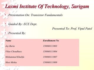
- 1. Laxmi Institute Of Technology, SarigamLaxmi Institute Of Technology, Sarigam • Presentation On: Transistor Fundamentals • Guided By: ECE Dept. Presented To: Prof. Vipul Patel • Presented By: Name Enrollnment No. Jay Baria 150860111003 Vikas Choudhary 150860111004 Mohammed Khalifa 150860111007 Meet Mehta 150860111009
- 2. IntroductionIntroduction • The basic of electronic system nowadays is semiconductor device. • The famous and commonly use of this device is BJTs (Bipolar Junction Transistors). • It can be use as amplifier and logic switches. • Transistors consists of three terminal: collector : C base : B emitter : E • Two types of Transistors : pnp and npn
- 3. Types of Transistors • Circuit Symbols There are two types of standard transistors, NPN and PNP, with different circuit symbols. The letters refer to the layers of semiconductor material used to make the transistor. Most transistors used today are NPN because this is the easiest type to make from silicon. If you are new to electronics it is best to start by learning how to use NPN transistors. The leads are labeled base (B), collector (C) and emitter (E).
- 4. Who Invented the Transistor? • In the mid 1940’s a team of scientists working for Bell Telephone Labs in Murray Hill, New Jersey, were working to discover a device to replace the then present vacuum tube technology. Vacuum tubes were the only technology available at the time to amplify signals or serve as switching devices in electronics. The problem was that they were expensive, consumed a lot of power, gave off too much heat, and were unreliable, causing a great deal of maintenance.
- 5. Transistors……. • A Transistor is an semiconductor which is a fundamental component in almost all electronic devices. Transistors are often said to be the most significant invention of the 20th Century. Transistors have many uses including switching, voltage/current regulation, and amplification - all of which are useful in renewable energy applications. • The transistor is one of the most important component used in electronics, even integrated circuits have many thousands of them within it. Many electronic products and their circuits rely on sensors in order to function, most sensors provide only a very small output current or voltage, it is necessary to amplify this current or voltage
- 6. Transistor ConstructionTransistor Construction • 3 layer semiconductor device consisting: • 2 n- and 1 p-type layers of material npn transistor • 2 p- and 1 n-type layers of material pnp transistor • The term bipolar reflects the fact that holes and electrons participate in the injection process into the oppositely polarized material • A single pn junction has two different types of bias: • forward bias • reverse bias • Thus, a two-pn-junction device has four types of bias.
- 7. Position of the terminals and symbol of transistor. • Base is located at the middle and more thin from the level of collector and emitter • The emitter and collector terminals are made of the same type of semiconductor material, while the base of the other type of material • Base is located at the middle and more thin from the level of collector and emitter • The emitter and collector terminals are made of the same type of semiconductor material, while the base of the other type of material
- 8. Transistor currents -The arrow is always drawn on the emitter -The arrow always point toward the n-type -The arrow indicates the direction of the emitter current: pnp:E B npn: B E IC=the collector current IB= the base current IE= the emitter current
- 9. • By imaging the analogy of diode, transistor can be construct like two diodes that connetecd together. • It can be conclude that the work of transistor is base on work of diode.
- 10. Transistor OperationTransistor Operation • The basic operation will be described using the pnp transistor. The operation of the pnp transistor is exactly the same if the roles played by the electron and hole are interchanged. • One p-n junction of a transistor is reverse-biased, whereas the other is forward-biased. Forward-biased junction of a pnp transistor Reverse-biased junction of a pnp transistor
- 11. • Both biasing potentials have been applied to a pnp transistor and resulting majority and minority carrier flows indicated. • Majority carriers (+) will diffuse across the forward- biased p-n junction into the n-type material. • A very small number of carriers (+) will through n-type material to the base terminal. Resulting IB is typically in order of microamperes. • The large number of majority carriers will diffuse across the reverse-biased junction into the p-type material connected to the collector terminal.
- 12. • Majority carriers can cross the reverse-biased junction because the injected majority carriers will appear as minority carriers in the n-type material. • Applying KCL to the transistor : IE = IC + IB • The comprises of two components – the majority and minority carriers IC = ICmajority + ICOminority • ICO – IC current with emitter terminal open and is called leakage current.
- 13. Common-Base ConfigurationCommon-Base Configuration • Common-base terminology is derived from the fact that the : - base is common to both input and output of the configuration. - base is usually the terminal closest to or at ground potential. • All current directions will refer to conventional (hole) flow and the arrows in all electronic symbols have a direction defined by this convention. • Note that the applied biasing (voltage sources) are such as to establish current in the direction indicated for each branch.
- 15. • To describe the behavior of common-base amplifiers requires two set of characteristics: - Input or driving point characteristics. - Output or collector characteristics • The output characteristics has 3 basic regions: - Active region –defined by the biasing arrangements - Cutoff region – region where the collector current is 0A - Saturation region- region of the characteristics to the left of VCB = 0V
- 17. • The curves (output characteristics) clearly indicate that a first approximation to the relationship between IE and IC in the active region is given by IC ≈IE • Once a transistor is in the ‘on’ state, the base-emitter voltage will be assumed to be VBE = 0.7V
- 18. • In the dc mode the level of IC and IE due to the majority carriers are related by a quantity called alpha α= IC = αIE + ICBO • It can then be summarize to IC = αIE (ignore ICBO due to small value) • For ac situations where the point of operation moves on the characteristics curve, an ac alpha defined by • Alpha a common base current gain factorcommon base current gain factor that shows the efficiency by calculating the current percent from current flow from emitter to collector.The value of α is typical from 0.9 ~ 0.998. E C I I E C I I ∆ ∆ =α
- 19. BiasingBiasing • Proper biasing CB configuration in active region by approximation IC ≈ IE (IB ≈ 0 uA)
- 20. Transistor as an amplifierTransistor as an amplifier
- 21. Simulation of transistor as anSimulation of transistor as an amplifieramplifier
- 22. Common-Emitter ConfigurationCommon-Emitter Configuration • It is called common-emitter configuration since : - emitter is common or reference to both input and output terminals. - emitter is usually the terminal closest to or at ground potential. • Almost amplifier design is using connection of CE duedue to the high gain for current and voltageto the high gain for current and voltage. • Two set of characteristics are necessary to describe the behavior for CE ;input (base terminal) and output (collector terminal) parameters.
- 23. Proper Biasing common-emitter configuration in active region
- 24. Input characteristics for a common-emitter NPN transistorcommon-emitter NPN transistor • IB is microamperes compared to miliamperes of IC. • IB will flow when VBE > 0.7V for silicon and 0.3V for germanium • Before this value IB is very small and no IB. • Base-emitter junction is forward bias • Increasing VCE will reduce IB for different values.
- 25. Output characteristics for a common-emitter npn transistor • For small VCE (VCE < VCESAT, IC increase linearly with increasing of VCE • VCE > VCESAT IC not totally depends on VCE constant IC • IB(uA) is very small compare to IC (mA). Small increase in IB cause big increase in IC • IB=0 A ICEO occur. • Noticing the value when IC=0A. There is still some value of
- 27. Beta (β) or amplification factoramplification factor • The ratio of dc collector current (IC) to the dc base current (IB) is dc beta (βdc ) which is dc current gain where IC and IB are determined at a particular operating point, Q-point (quiescent point). • It’s define by the following equation: 30 < βdc < 300 2N3904 • On data sheet, ββdcdc==hhFEFE with hh is derived from ac hybrid equivalent cct. FE are derived from forward-current amplification and common-emitter configuration respectively.
- 28. • For ac conditions an ac beta has been defined as the changes of collector current (IC) compared to the changes of base current (IB) where IC and IB are determined at operating point. • On data sheet, βac=hfe • It can defined by the following equation:
- 30. Relationship analysis between αα and ββ
- 31. Common – Collector ConfigurationCommon – Collector Configuration • Also called emitter-follower (EF). • It is called common-emitter configuration since both the signal source and the load share the collector terminal as a common connection point. • The output voltage is obtained at emitter terminal. • The input characteristic of common-collector configuration is similar with common-emitter. configuration. • Common-collector circuit configuration is provided with the load resistor connected from emitter to ground. • It is used primarily for impedance-matching purpose since it has high input impedance and low output impedance.
- 32. Notation and symbols used with the common-collector configuration: (a) pnp transistor ; (b) npn transistor.
- 33. • For the common-collector configuration, the output characteristics are a plot of IE vs VCE for a range of values of IB.
- 34. Limits of OperationLimits of Operation • Many BJT transistor used as an amplifier. Thus it is important to notice the limits of operations. • At least 3 maximum values is mentioned in data sheet. • There are: a) Maximum power dissipation at collector: PCmax or PD b) Maximum collector-emitter voltage: VCEmax sometimes named as VBR(CEO) or VCEO. c) Maximum collector current: ICmax • There are few rules that need to be followed for BJT transistor used as an amplifier. The rules are: i) transistor need to be operate in active region! ii) IC < ICmax ii) PC < PCmax
- 35. Note: VCE is at maximum and IC is at minimum (ICmax=ICEO) in the cutoff region. IC is at maximum and VCE is at minimum (VCE max = VCEsat = VCEO) in the saturation region. The transistor operates in the active region between saturation and cutoff.
- 36. Refer to the fig. Step1: The maximum collector power dissipation, PD=ICmax x VCEmax (1) = 18m x 20 = 360 mW Step 2: At any point on the characteristics the product of and must be equal to 360 mW. Ex. 1. If choose ICmax= 5 mA, subtitute into the (1), we get VCEmaxICmax= 360 mW VCEmax(5 m)=360/5=7.2 V Ex.2. If choose VCEmax=18 V, subtitute into (1), we get VCEmaxICmax= 360 mW (10) ICmax=360m/18=20 mA
- 37. Derating PDerating PDmaxDmax • PDmax is usually specified at 25°C. • The higher temperature goes, the less is PDmax • Example; • A derating factor of 2mW/°C indicates the power dissipation is reduced 2mW each degree centigrade increase of temperature.
- 38. Transistor Specification SheetTransistor Specification Sheet
- 40. Transistor Testing 1. Curve Tracer Provides a graph of the characteristic curves. 2. DMM Some DMM’s will measure βDC or HFE. 3. Ohmmeter