SlideShare a Scribd company logo
1 of 23
Download to read offline
C SCI 360 Computer Architecture 3 Prof. Stewart Weiss
Storage and I/O
Storage and I/O
The standard for dependability is higher for storage systems than it is for computation. It is one
thing for a processor to hang or even crash, but another if a hard disk fails. The former case is an
inconvenience but the latter might mean data loss. Therefore, I/O systems place greater
emphasis on:
• dependability
• cost
• expandability
than they do on performance. Performance is more complex to analyze for storage and I/O
devices than it is for processors. It depends on several factors, including:
• device characteristics
• connection between device and system
• memory hierarchy
• operating system
There is a wide range of I/O devices, from keyboards and mice to magnetic and optical disks to
wireless network cards. One way to organize this diversity is by characterizing devices according
to three criteria:
Behavior: input/output or both (storage)
Partner: human or machine
Data rate: peak data rate (maximum rate at which transfers between device and main
memory
1
Figure 1: Typical collection of I/O devices
C SCI 360 Computer Architecture 3 Prof. Stewart Weiss
Storage and I/O
Assessing Performance
Should performance be measured by
• system throughput (jobs completed per unit time), or
• response time?
Throughput can be measured by bandwidth, either
(1) number of completed I/O operations per unit time, or
(2) number of bytes transferred per unit time
Examples.
1. Transaction processing systems such as on-line commerce applications and on-line
banking systems have to handle a large number of small transactions, so (1) is a better
measure than (2).
2. A system for delivering streaming video, on the other hand, is better measured by the
volume of bytes transferred per unit time (2) than by the number of completed
transactions.
Throughput is not always the best measure. Sometimes response time is more important. Often
not just the mean response time, but the standard deviation of response times (indicates how
reliable the system is). For single-user workstations, response time is typically the most
important performance measure.
Sometimes both are equally important:
3. ATM networks, file servers, and web servers must have short response times for their
customers and must also process large amounts of data quickly.
Dependability, Reliability, and Availability
Dependability is the quality of a system such that reliance can be placed on its service. The
service delivered by a system is its observed actual behavior as perceived by another system that
interacts with it. The other system may be a machine, a person, or both.
Dependability is therefore dependent on a reference point, since it may be different to different
observers. To remove this subjectivity, there needs to be a reference standard, called a system
specification, that specifies expected behavior.
When such a specification exists, one can define:
1. Service accomplishment -- the state during which service is being delivered (meets
specification).
2. Service interruption -- the state in which the delivered service is different from the
specified service. This could mean no service at all, or service that fails to meet the
specification.
A failure is a transition from state 1 to state 2. A transition from state 2 to state 1 is called a
restoration.
2
C SCI 360 Computer Architecture 3 Prof. Stewart Weiss
Storage and I/O
Failures can be permanent or intermittent. Intermittent failures are harder to diagnose.
Reliability is a measure of continuous service accomplishment. Equivalently, it can be measured
by the mean time to failure (MTTF). (The amount of time it is available without interruption,
on average.)
Annual failure rate (AFR) is related -- it is the average number of failures per year, i.e., the
average number of devices, that would fail in a year for a given MTTF.
Service interruption is measured by how long a system is unavailable, which is characterized by
the mean time to repair (MTTR).
Mean time between failures (MTBF) is the sum of MTTF and MTTR. You can think of it as the
time to the next failure plus the time it takes to repair that failure and bring the system back to
the available state. This sum is the time from the last time it was brought up to the next time it
was brought up.
Availability is defined as
Availability = MTTF/ (MTTF + MTTR)
Then 0 <= Availability <= 1.0. It is the fraction of time that a system is achieving service
accomplishment.
To improve MTTF, either one improves the quality of the components or makes the entire
system more fault tolerant. A system is fault tolerant if a failure does not lead to unavailability.
A fault is a failure of a component.
Hence MTTF can be improved by either:
1. Fault avoidance -- make the components better do that they do not fail as frequently.
2. Fault tolerance -- use redundancy to allow service to continue to meet the specification
despite the occurrence of faults. RAID is an example of building
fault tolerance into a storage system.
3. Fault forecasting -- predicting the presence and creation of faults, both hardware and
software, to allow for replacing it before the failure occurs.
3
Figure 2: Summary of studies of causes of failure, from
Ptterson/Hennessey
C SCI 360 Computer Architecture 3 Prof. Stewart Weiss
Storage and I/O
Disk Storage
Magnetic Disks
All magnetic disks have the following properties in common:
• One or more rotating platters (they rotate in unison)
• Magnetic coated surface
• Movable read/write head
• Nonvolatile
• Rotation speed from 5400 to 15000 RPM
There is some important terminology to remember regarding the structure of a magnetic disk
drive:
• A platter is one disk of a set of one or more coaxial disks.
• A surface is one of the two surfaces of any platter. Each surface is divided into a set of
concentric circles, called tracks.
• A track is one of the concentric rings on a surface on which the data is recorded.
• A sector is the consecutive sequence of bits on a track within a pre-specified arc of the
circle.
• A cylinder is the set of all tracks under the read/write heads, on all surfaces, at a given
time
Tracks are not necessarily divided into the same number of sectors. Inner tracks may have fewer
sectors than outer tracks. The idea is to keep the bits uniformly spaced in each track. This is
called zone bit recording (ZBR).
Performance Costs
To perform a read or a write on a disk, three steps must be taken:
1. The read/write heads must be moved in or out until they are positioned over the
appropriate track. This is called seeking.
2. The head then waits until the right sector has moved under the head.
3. The data is transferred to or from the disk.
Each of these steps has an associated cost in terms of time:
• Seek time The amount of time for the heads to move to the right track
• Rotational latency The time spent waiting for the right sector to rotate under the
heads. (Also called rotational delay.)
• Transfer time The time to transfer a block of bits, which depends upon sector
size, rotation speed, and the recording density of the track.
4
C SCI 360 Computer Architecture 3 Prof. Stewart Weiss
Storage and I/O
In addition, there is a fourth component to the overall time overhead that is related to the disk
controller. The disk controller is the disk's processing unit and is responsible for receiving
instructions and data and controlling the activities of the disk. The controller's execution time is
another factor in the overhead of disk I/O:
• Controller overhead The time spent by controller to initiate and finalize I/O transfers.
The complication in true performance estimation is that modern controllers come with very large
caches and do anticipatory caching of sectors. Transfer time from the cache to the processor is
much smaller because there is no mechanical operation involved; the data are read from or
written to the cache directly.
Common Measures
Disk manufacturers usually report minimum seek time, maximum seek time, and average seek
time. Average seek time depends upon many factors and so is not always useful. Typical
average seek times are between 3 ms and 13 ms.
Average rotational latency is between
½ rotation / minimum rotations per sec = 0.5 /5400 RPM
= 0.5/90 sec = 0.0056 sec = 5.6 ms
and
½ rotation / maximum rotations per sec = 0.5 /15000 RPM
= 0.5/250 sec = 0.002 sec = 2.0 ms
Transfer time depends on sector size, recording density, and rotation speed. Typical transfer rates
are between 125 MB/sec and 200 MB/sec, but when transfers are measured from the cache, they
can be as much as 400 MB/sec.
Example
What is the average time to read or write a 512 byte sector for a disk rotating at 5400 RPM,
given advertised
• average seek time = 12 ms
• transfer rate = 5 MB/sec
• controller overhead = 2 ms
Time to read a 512 byte sector is
= seek time + rotational latency + transfer time + controller overhead
= 12 ms + 0.5/(5400/60) sec + 512 bytes/(5 MB/sec) + 2 ms
= 12 ms + 5.6 ms + 0.1 ms + 2 ms
= 19.7 ms
5
C SCI 360 Computer Architecture 3 Prof. Stewart Weiss
Storage and I/O
Rotational delay can be the dominating cost if seek time is much less.
Flash Storage
Flash memory is a type of EEPROM (electrically erasable programmable read-only memory)
that has grown in popularity because:
• it is durable (resistant to shock)
• it is compact
• it is power-efficient
• it has much smaller latency than hard disks
In addition, its capacity is usually large enough for many applications (cameras, phones, media
players) but is available in small capacities for small devices. Because of these features, it is the
first technology that is competitive with magnetic disks in the secondary storage market.
There are two types of flash memory: NOR flash and NAND flash. The original technology was
NOR flash. NOR flash provided random access memory. NAND flash provided much more
storage capacity but could only read and written in blocks. In addition it is much less expensive
than NOR flash.
Characteristics NOR flash NAND flash
Typical use BIOS USB key
Minimum access size (bytes) 512 2048
Read time (msec) 0.08 25
Write time (msec) 10.00 1500 to erase + 250
Read bandwidth (MB/sec) 10 40
Write bandwidth (MB/sec) 0.4 8
Wear-out (writes per cell) 100,000 10,000 to 100,000
Best price/GB (2008) $65 $4
Table 1: NOR versus NAND flash memory comparison (from Paterson & Hennessey).
The limiting factor is that bits wear out with writes over time. The table above shows that
NAND flash will wear out faster than NOR flash. Flash drive controllers reduce the chance of
wear-outs by trying to distribute writes uniformly across the memory. They do this by moving
logical blocks that have been written a lot to different physical blocks. This is called level
wearing.
6
C SCI 360 Computer Architecture 3 Prof. Stewart Weiss
Storage and I/O
Connecting Processors, Memory, and I/O Devices
A bus is a shared communication path whose purpose is to allow the transfer of data among the
devices connected to it. A bus includes address, control, and data lines as well as lines needed
to support interrupts and bus arbitration. Control lines include a read/write line.
A bus protocol is a set of rules that govern the behavior of the bus. Devices connected to the bus
have to use these rules to transfer data. The rules specify when to place data on the bus, when to
assert and de-assert control signals, and so on.
Among methods of interconnecting components of a computer system, buses are
• versatile
• low-cost
• a major bottleneck
Bus speed is limited by:
• bus length
• number of attached devices
Buses can be synchronous or asynchronous; synchronous buses use a clock to control transfers,
whereas asynchronous buses do not. This is discussed further below.
Because of clock skew and signal reflection, it is difficult to design buses with many parallel
wires at high speed. Clock skew is the difference in absolute time between when two state
elements see a clock edge. Clock skew arises because the clock signal will often use two
different paths, with slightly different delays, to reach two different state elements. When the
length of the wires is long and clock speeds are fast, skew can become a problem. The reflection
of the clock signal is also a problem as clock speeds get faster.
Buses are gradually being replaced by serial point-to-point interconnection networks with
switches. Nonetheless, we begin with a brief overview of buses.
Bus Types
Different kinds of buses are used to connect different parts of a computer system to each other.
Processor-Memory Bus
These are sometimes called processor buses. They are short, high speed buses, usually designed
for a specific memory and processor to maximize bandwidth. They can be used when all devices
that can be attached are known in advance and have known characteristics. Typically these are
proprietary buses.
I/O Bus
I/O buses have varying length and usually allow many different kinds of devices with varying
speeds and data block sizes to be attached. I/O buses may be connected to the processor bus via a
7
C SCI 360 Computer Architecture 3 Prof. Stewart Weiss
Storage and I/O
bridge or a separate controller interface, but usually they are connected to what is often called a
system, or backplane, bus, described below. I/O buses are almost always standard, off-the-
shelf components. Examples include SCSI, USB, PCI Express, Serial ATA (SATA), and Serial
attached SCSI (SAS) .
Backplane, or System, Bus
Most modern computers use a single, general-purpose bus to interconnect a variety of internal
devices, including network interface cards, DMA controllers, and hard disk drives. These buses
used to be called backplane buses but are now often called system buses. Usually, I/O buses are
connected to the system bus, which in turn connects to the processor bus via a bridge.
Connection Basics
In any transfer operation, there are two parts -- sending the address and sending or receiving
data. The device initiating the request is called the master, and the one receiving the request is
called the slave. The processor is often the master, but memories can be masters as well. When
it comes to buses, the direction of the operation is defined from the perspective of memory: A
read operation is one that transfers data from memory to a device, and a write operation
transfers data from a device into memory. To clarify the language, we can avoid using read and
write and instead use input and output. Input refers to transfers from devices into memory, and
output refers to transfers from memory to devices.
Synchronous Buses
A synchronous bus has a clock line accessible to all attached devices, and a clock that generates
uniform pulses on the line. A bus cycle is the interval between one or more consecutive pulses.
The simplest synchronous bus uses a single long clock cycle for data transfers and ensures that
all data transfers take one clock cycle. The cycle is long enough to accommodate all devices.
This design is inefficient because all transfers take as long as the slowest device. Sometimes
instead of a single cycle, all transfers take a fixed number of cycles greater than 1.
More general synchronous buses use a higher frequency clock rate and allow different devices to
use different numbers of clock cycles for a single transfer. One device might respond after two
clock cycles and another might require five. In all synchronous buses, the bus protocol is based
upon the use of clock cycles exclusively to coordinate transfers of data.
Example
A simplistic (and unrealistic) protocol to input a word from memory to the processor :
transmit a read request on the R/W control line and address on data line
wait 5 clock cycles;
store data from memory into processor location
8
C SCI 360 Computer Architecture 3 Prof. Stewart Weiss
Storage and I/O
Advantages
• Relatively simple control logic
• Usually fast, because the protocol uses little bus overhead
Disadvantages:
• Does not work if bus length is too great because clock skew (clock signals arriving at
different times from different devices) can corrupt logic.
• Must be designed to accommodate the slowest device.
• Adding new devices complicates the design.
Asynchronous Buses
Most of the popular buses in use in 2011 are asynchronous, including USB 2.0, PCI Express
(PCIe), Serial ATA (SATA), Serial Attached SCSI (SAS) and Firewire.
An asynchronous bus is not clocked. Instead, devices communicate by exchanges messages
with each other. These messages are called handshakes. Because it is not clocked, it is a more
versatile bus, but the complex, handshaking protocol can consume more overhead.
Handshaking is like the please-and-thank-you protocol that people use in everyday life. Each
party in a communication expects a certain response to its message and until it receives that
response, it does not advance to its next logical state. Think about a telephone call. When you
call, you expect the person responding to answer with some verbal message such as “hello” or
9
Figure 3: Traditional I/O Interconnections and Buses
Processor Memory
Bridge
ProcessorBus
PCIBus(systembus)
SCSI
Controller
Ethernet
Interface
USB
Controller
SCSIbus
SCSIDisk
Controller
Printer Joystick
CD-ROM
Controller
C SCI 360 Computer Architecture 3 Prof. Stewart Weiss
Storage and I/O
“this is so-and-so.” That person expects you to reply with a greeting in return, and if no reply is
forthcoming, he or she will hang up.
Advantages
• Handshake eliminates need for synchronization of clocks
• Can be unlimited length
• Can add devices or change delays without redesign of bus
• Can support a wide variety of devices
Disadvantages
• Generally slower than synchronous buses for short lengths
The I/O Interconnects of the x86 Processors
The I/O system depicted in Figure 4 is typical of that of all x86 processors. There are two
controller hubs, called the north bridge and the south bridge. The processor connects to
memory and peripheral devices via these hubs.
The north bridge is the memory controller hub, and connects the processor to the memory, the
south bridge, and sometimes the graphics card (via a PCIe bus.) The south bridge is the I/O
controller hub and connects the processor to all I/O devices, through a number of different kinds
of attached buses such as the USB, PCI, SATA and so on.
10
Figure 4: Schematic organization of the Intel 5000P I/O system (from
[Paterson/Hennessey])
C SCI 360 Computer Architecture 3 Prof. Stewart Weiss
Storage and I/O
Some processors, such as the AMD Opteron X4, incorporate the north bridge into the processor
ship instead of its being a separate chip.
Interfacing I/O Devices to the Processor, Memory, and OS
This section answers the following questions:
• How is an I/O request transformed into device-specific commands?
• How is an I/O request actually communicated to the I/O device?
• How is data transferred to or from the memory?
• What are the respective roles of the application level software, the operating system, and
the hardware?
The answers to these questions will vary depending upon how the computer system is designed
to be used. Most modern computers and operating systems support multi-processing, interactive
use, and multiple users. To provide these features, the operating system must perform under the
following constraints:
• The I/O system is shared among multiple processes.
• If processes are allowed to control devices directly, then throughput and response time
will not be under the control of the operating system, and the computer system will
perform poorly.
• If user processes are required to issue I/O requests directly to devices, then the
programming task becomes much more tedious for the software engineer.
• I/O requests should be handled by the operating system, and the operating system must
determine when the requested I/O has completed.
• Because I/O is handled by the operating system, the operating system must provide
equitable access to I/O resources and device abstraction.
To satisfy these constraints, the operating system must be able to communicate with devices and
prevent user programs from communicating with these devices. There are three differernt types
of communication:
• Issuing commands to devices (e.g., read, write, seek, start, stop)
• Receiving notifications when devices need attention (e.g., I/O completion, error, load
media)
• Transferring data between memory and a device.
The most common paradigm used in operating systems is a multi-layered approach to resources.
Users make requests for I/O to application software. Application software translates these
requests into calls to the operating system. The device drivers are the operating system’s lowest
level software; they are really two parts. One part issues I/O commands to the devices. The other
part responds to signals sent by the device to the processor when they need attention. Together
they maintain the queues needed to coordinate the requests. The operating system notifies
applications when the I/O is completed.
11
C SCI 360 Computer Architecture 3 Prof. Stewart Weiss
Storage and I/O
Giving Commands to I/O Devices
In order for the processor to issue a command to an I/O device, it has to be able to address the
device and it has to be able to deliver one or more commands to it. There are two different
methods of addressing devices: memory-mapped I/O and special I/O instructions.
Memory-Mapped I/O
In memory-mapped I/O, parts of the address space are reserved for I/O device ports. Device port
locations are mapped to specific memory addresses in such a way that when the processor
accesses these locations, it is really accessing the device ports. Ordinary instructions are written
to these addresses in order to perform I/O as if they were data. When the processor references an
address in this special part of the address space, the memory controller ignores the address;
instead the hardware translates this to the corresponding I/O device register. The I/O device
controller receives the data and interprets it as a command which it can then carry out.
Certain addresses are used for specific commands. For example, one address might be for reads
from the device and another, for writes. In the Intel IA-32 instruction set, the identifiers DATAIN
and DATAOUT are mnemonic names for memory addresses that are mapped to I/O device
registers. The ordinary MOV machine instruction
MOV AL, DATAIN
moves a character from the device register into register AL and the instruction
MOV DATAOUT,AL
moves a character from register AL to the device register. An example of an IA-32 I/O program
to read from the keyboard and echo the characters on the screen is shown below. IA-32 is a 32-
bit Intel instruction format.
Example (Intel IA-32 instructions)
In the Intel-32 instruction set, there are two device status registers, INSTATUS and
OUTSTATUS. The following program assumes that the keyboard synchronization flag is stored
in bit 3 of INSTATUS and the display synchronization flag is stored in bit 3 of OUTSTATUS.
LEA EBP,LOC # Register EBP points to LOC, the memory area
READ: BT INSTATUS,3 # INSTATUS bit 3 is set if there is data in
JNC READ # DATAIN; this loops waits for data
MOV AL,DATAIN # Transfer char into register AL
MOV [EBP],AL # Transfer AL contents to address in EBP
INC EBP # and increment EBP pointer
ECHO: BT OUTSTATUS,3 # Wait for display to be ready
JNC ECHO
MOV DATAOUT,AL # Send char to display
CMP AL,CR # If not carriage return,
JNE READ # read more chars
Notes.
• LEA reg, addr is an instruction to load the address addr into the pointer register reg.
12
C SCI 360 Computer Architecture 3 Prof. Stewart Weiss
Storage and I/O
• BT is a bit-test instruction. It loads the value in bit 3 of the specified register into the
carry bit; JNC will branch if the carry bit is 0.
Figure 5 illustrates the basic structure of the connections when memory-mapped I/O is used. The
four bus lines are for data, addresses, a read signal, and a write signal. Figure 6, in contrast,
shows the structure when special I/O instructions are used. In this case there are separate control
lines from the CPU to memory and from the CPU to the I/O devices.
Figure 5: Lines used in memory-mapped I/O
Communicating Via Special I/O Instructions
In isolated I/O, or I/O-mapped I/O, the processor has special instructions that perform I/O and
a separate address space for the I/O devices. In isolated I/O, the same address lines are used to
address memory and the I/O devices; the processor asserts a control line to indicate that the I/O
devices should read the address lines. All I/O devices read the address but only one responds. For
example, in the IA-32 instruction format,
IN REGISTER,DEVICE_ADDR
and
OUT DEVICE_ADDR,REGISTER
are the input and output instructions respectively. DEVICE_ADDR is an 8-bit address, and
REGISTER is either AL or EAX. Some instruction sets, such as the IA-32, support both
memory-mapped and isolated I/O.
In Figure 6 the separate physical lines for communicating with the I/O devices and memory are
labeled READIO and WRITEIO to symbolize that special commands would be issued to use
these lines.
13
I/O
DeviceB
I/ODeviceA
Memory
I/OPort
1
I/OPort
2
I/OPort
3
CPU
C SCI 360 Computer Architecture 3 Prof. Stewart Weiss
Storage and I/O
Figure 6: Isolated I/O (using special I/O instructions)
Methods of Controlling I/O
There are three basic methods of controlling I/O and interacting with devices: polling, interrupt-
driven I/O, and direct memory access (DMA). These are described in turn.
Polling (Program-controlled I/O)
The program above that reads from the keyboard and echos the characters to the screen is an
example of polling. In polling, every byte of data is transferred under the control of the CPU.
An I/O program issues instructions to the I/O device to transfer the data. The data is transferred
to or from memory by the program. On a read, for example, the program must request the input
operation and then repeatedly test the status of a bit or register to see if the input is available. It
does this in a “busy-waiting” loop in which it “polls” the device to see if it is ready. In effect, it
is the nagging child on the long trip, “are we there yet, are we there yet, are we there yet,…”
until at long last we have arrived. This method is appropriate if the performance requirements are
not great and the hardware does not support the other methods. In general, it is wasteful of
computing cycles.
In certain situations, polling is a good solution, such as when I/O rates are completely
predetermined. In this case, the processor knows exactly when the data will be ready, so the
overhead is predictable. The disadvantage of polling is that the processor is completely
consumed with the I/O, spinning in idle cycles waiting for the I/O device to finish, which is a
waste of valuable CPU cycles, especially if the frequency of polling is great. The following
example demonstrates this.
Example.
Assume that a computer has a 500 MHz clock, and that the instructions in the operating system
that are executed to perform the polling operation use 400 clock cycles. What is the overhead to
poll each of the following three devices, with the stated characteristics?
1. Mouse: can produce an event 30 times per second.
14
Memory
I/O
DeviceB
DATA
ADDR
WRITE
WRITEIO
I/ODeviceA
I/OPort
1
I/OPort
2
I/OPort
3
READIO
CPU
READ
C SCI 360 Computer Architecture 3 Prof. Stewart Weiss
Storage and I/O
2. Floppy disk: can transfer 2-byte blocks at a rate of 50KB/second.
3. Hard disk: can transfer 4-word blocks at a rate of 4MB/second.
Solution.
The operating system uses 400 2ns clock cycles per polling operation, or 800 ns.
Mouse: 30*800 ns /second = 0.000024 or 0.0024%.
Floppy Disk: 50KBytes/sec at 2 bytes per transfer implies that it performs 25,000 transfers per
second. The overhead is 25,000*800 ns/second = 0.02 or 2%.
Hard Disk: 4MB/second at 4 words per transfer implies that it transfers 250,000 times per
second. The overhead is 250,000*800 ns/ second = 0.2 or 20%.
This shows that the faster the device, the more overhead is involved in polling as a means of
controlling I/O.
Interrupt-driven I/O
An alternative to programmed I/O is In interrupt-driven I/O. In interrupt-driven I/O, a program
running on the processor issues an I/O command to a device and then goes into a waiting state.
Another process is run on the processor while the I/O is carried out. When the I/O completes, the
I/O device sends a signal, called an interrupt, to the processor. This signal is like an exception
except that it is asynchronous.
This requires adding more signals to the bus and more logic to the I/O devices to allow them to
notify the CPU when the device is ready for a new I/O operation, or when an I/O operation is
complete. There are various ways to arrange this, some more complex and flexible than others.
Regardless of the method, it has to provide a means of deciding which device caused the
interrupt.
Figure 7: Interrupts with a single interrupt request line
The simplest scheme is a single control line on the bus, usually denoted INTR. All devices share
this line. The line is the logical OR of the interrupt requests of the attached devices. If any device
has issued an interrupt, the processor receives the signal. The processor then has to determine
15
CPU
Interrupt
Flip-Flop
Device1 Device2 Device3
InterruptRequestLineINTR
INTA
C SCI 360 Computer Architecture 3 Prof. Stewart Weiss
Storage and I/O
which device issued the request, which it does by polling the status registers of the devices. Once
it has determined which device issued the request, it can initiate the transfer of data.
If interrupts arrive at the same time, the processor has to decide which to accept. Generally, it
does this by assigning priorities to the devices. With a single interrupt line, priorities can be
assigned by using a daisy chain scheme like the kind used for bus arbitration. In a daisy chain,
the devices are arranged in a sequence such that each device is connected to the next one and
passes messages down the line if they are not addressed to it. That is the purpose of the INTA
line in Figure 7, which runs through the devices. The processor sends an Interrupt
Acknowledge signal through the line. The closest device that has an outstanding interrupt request
intercepts the signal.
Another solution is to use a multiple-line interrupt system. In this case each device has a
dedicated INTR line and a dedicated INTA line. This makes it easy to decide which device
caused the interrupt. The lines run into a priority arbitration circuit in the CPU. The CPU chooses
the highest priority interrupt.
Handling Interrupts
When an interrupt occurs, the CPU needs to execute the subroutine that handles, or services, the
interrupt. To do this, the contents of some of its registers must be saved. Modern processors
typically allow two types of interrupts, one that forces a save of the entire register set, and
another that saves only a minimal set of registers. The latter is the more efficient solution since
only a few registers are saved, and the subroutine can choose to save whatever other registers it
needs to in order to execute. This is faster than saving all registers, and avoids unnecessary work
if there is no need to save them. The registers may be saved in special dedicated storage, or put
on the system stack. The interrupt service routine (ISR) runs, saves whatever CPU state it must,
and on completion, either the previous instruction sequence is resumed, or the scheduler is run
to pick a different process to run.
How does the operating system know which ISR to execute? The answer is that once it knows
which device caused the interrupt it knows which subroutine to run. In vectored interrupts, there
is a portion of memory that contains an array, i.e., a vector, each of whose cells is the starting
address of an interrupt service routine (ISR). Each device has an entry in this vector. When an
interrupt occurs, the address of the device is used as an index into this array, and the starting
address of the interrupt service routine is automatically loaded, once the registers have been
saved.
There are other issues related to interrupts. They include:
1. Should interrupts be disabled while an interrupt service routine is running? If so, is the
interrupt lost, or is it just that the response is delayed?
2. If not disabled, what happens if an interrupt occurs while an interrupt service routine is
running?
There are various answers to these questions, depending on the complexity of the system. There
are usually two registers, a Cause Register and a Status Register, used to solve the first
16
C SCI 360 Computer Architecture 3 Prof. Stewart Weiss
Storage and I/O
question. The Cause Register has a bit for each different interrupt. If an interrupt occurs, the bit
is set to 1, otherwise it is 0. The Status Register bits are used as an interrupt mask. If an
interrupt is enabled, there must be a 1-bit in the corresponding position in the Status Register.
AND-ing the two registers gives the set of enabled interrupts that have occurred.
The mask can be used to set the interrupt priority level of the processor by a left-to-right ordering
of the mask bits. If an interrupt occurs whose bit is to the left of another one, it has higher
priority. By turning off all bits to the right of a given bit, the processor masks all lower level
interrupts than a given level. If an interrupt occurs that is lower priority than the current priority
level, it is ignored. If one occurs that is a higher or equal priority, the currently running process is
preempted in favor of the interrupt service routine that handles the new interrupt, regardless of
what it was doing. Each device has an associated priority level, and the ISR for that device runs
at that priority level. For example, the power supply can send an interrupt if it senses an
impending loss of power. This is the highest priority level on many machines. The system timer
is also very high priority; it must keep accurate time and uses very little CPU time when it runs,
so it is reasonable to allow it to run whenever it needs to, which is on the order of 60 times per
second.
Overhead
The overhead of interrupts is much lower than that of program-controlled I/O. To illustrate,
consider the hard disk from the preceding example, which could transfer 4-word blocks at a rate
of 4 MB/second. Suppose that the operating system needs 500 clock cycles of processing time to
handle an interrupt and that the disk is only busy 5% of the time.
For each of the 250,000 transfers per second that the disk generates, the interrupt service routine,
uses 500 clocks * 2 ns/clock = 1000 ns. Since it is busy 5% of the time, the overhead is 5% of
250,000 transfers * 1000 ns per transfer per second = 0.05 * 250,000,000 ns per second =
12,500,000 ns/second , which is 1.25%. Recall that polling used 20% of the CPU time, so this is
93.75% reduction in overhead (1.25/20 = 0.0625, so 1.25% is 6.25% of 20%.)
17
C SCI 360 Computer Architecture 3 Prof. Stewart Weiss
Storage and I/O
Direct Memory Access (DMA)
Direct Memory Access (DMA) is a method of transferring data at a very high bandwidth with
low overhead. The processor, under program control, effectively authorizes the a special device
to take charge of the I/O transfers to memory, allowing it to be the bus master until the I/O is
completed. A device with this capability is called a DMA controller.
Figure 8: Circuitry for DMA interface
DMA significantly reduces the involvement of the processor in data transfers between memory
and I/O devices. A DMA controller is an I/O processor that has the ability to communicate
directly with memory, transferring large blocks of data between memory and the I/O devices to
which it is attached. It achieves this because it is attached to the processor-memory bus on one
side, and either an I/O bus or a dedicated device on the other, and it can be bus master on the
memory bus. Typically, a single DMA controller will service multiple I/O devices. Certain
devices, usually high-speed devices such as hard disks, CD-ROM drives, or network interfaces,
may be equipped with DMA controllers. For example, a SCSI bus controller will have a DMA
controller in its interface, making it possible for all devices on the SCSI bus to transfer data
directly to or from memory with little CPU involvement.
A program running on the CPU will give the DMA controller a memory address, the number of
bytes to transfer, and a flag indicating whether it is a read or a write. It will also give it the
address of the I/O device involved in the I/O. The DMA controller becomes the bus master on
the memory bus. If it is an input operation, the device will then start sending data to the DMA
18
Main
Memory
IOAR
I/O
Address
Register
Data
Counter
IODR
I/OData
Register
Control
Unit
DMA
Controller
Address
Register
Register
File
Control
UnitCPU DMAAcknowledge
Data
Address
Control
DMARequest
System
Bus
I/O
Devices
C SCI 360 Computer Architecture 3 Prof. Stewart Weiss
Storage and I/O
controller, which will buffer the data, and store it in successive memory locations as it becomes
available. If it is an output operation, it buffers the data from memory and sends it to the I/O
device as it becomes ready to receive it. In effect, it does what the CPU would do, but the CPU
is free to do other things in the meanwhile. Figure 8 depicts the circuitry in a typical DMA
controller interface.
The typical sequence of operations in an input transfer would be:
1. The CPU executes two instructions to load the IOAR and the Data Counter. The IOAR gets
the start address in memory of the first byte to be stored and the Data Counter gets a count
of the number of bytes to be transferred.
2. When the DMA controller is ready, it activates the DMA request signal.
3. The CPU relinquishes control of the bus and activates DMA Acknowledge as part of the
handshake.
4. The DMA controller begins the transfer of data to memory using a hardware loop to update
the IOAR and Data Counter.
5. If the I/O device is not ready, but the transfer is not complete, the DMA controller
relinquishes the bus so that the processor can use it.
6. If the I/O device was not ready and it becomes ready, the DMA controller re-acquires the bus
in the same way it did in above.
7. When the Data Counter reaches 0, the DMA controller releases the bus and sends an
interrupt to the CPU.
Because the DMA controller owns the bus during a transfer, the CPU will not be able to access
memory. If the CPU or the cache controller needs to access memory, it will be delayed. For
small data transfers this may be acceptable, but not for large transfers, because it defeats the
purpose of using DMA in the first place. Therefore, DMA controllers usually operate in two
modes, one for small transfers and one for larger transfers, in which "cycle-stealing" is allowed.
In cycle-stealing, the CPU is allowed to interrupt the DMA transfer and acquire the bus.
DMA Overhead Example
Suppose that a system uses DMA for its hard disk. The system characteristics are:
1. System Clock: 500 MHz (2 ns per cycle)
2. Hard Disk can transfer at 4MB/second using an 8KB block size.
3. 1000 clock cycles are used in the CPU to setup the I/O and 500 clock cycles are used
afterwards in the CPU. What is the overhead of DMA transfers?
Each transfer takes 8KB / ( 4MB/ second) = 0.002 seconds (2 ms). Thus there are
1.0 / 0.002 = 500 transfers per second.
If the disk is busy then it takes (1000 + 500) * 2 ns per transfer, which is 3000 ns per transfer.
Since there are 500 transfers per second, the total overhead is 500*3000 ns per second, or 1.5 ms
per second, which is 0.15%.
19
C SCI 360 Computer Architecture 3 Prof. Stewart Weiss
Storage and I/O
DMA and Virtual Memory
In a system with virtual memory, DMA poses a problem – should the DMA controller use virtual
or physical addresses? If it uses physical addresses, then it cannot perform reads or writes that
cross page boundaries. To see this, imagine that pages are each 1 KB. If the DMA controller tries
to write 3KB of data, then it will write into 3 or 4 physical pages. These pages may not belong to
the same process, and may not be logically adjacent, and should be placed in the logically correct
memory locations. On the other hand, if it uses virtual addresses, it will need to translate every
address, slowing things down considerably and requiring a large RAM of its own. One solution
is for the DMA controller to keep a cache of translations in its memory and update it using a
replacement strategy such as LRU.
This is still inadequate because the page translations it has may go stale if the processor updates
the page tables independently. For DMA to work properly, the processor must be prevented
from changing the page tables during a DMA transfer.
DMA and Cache
DMA also creates problems with the cache. If the DMA controller is reading data directly from
the disk into memory, then cache blocks may become stale, because the cache blocks will not be
consistent with their corresponding memory blocks, which are newer. This is called the stale
data problem. Similarly, the DMA controller might read from memory and get stale data
because the system has a write-update cache that has not yet been flushed to memory. There are
a few solutions:
• Route all I/O through the cache.
• Flush the cache for I/O writes and invalidate it for I/O reads.
To make this efficient, special hardware is provided for flushing the cache.
I/O Performance Measures
Remember that I/O performance can be measured by throughput or response time or a
combination of both. Which we choose depends upon how the system will be used. Over time,
computer scientists have developed collections of programs called benchmarks that are run on
systems to measure their performance. The benchmarks are designed for specific purposes, such
as to measure the performance of a transaction processing system, or a supercomputer, or a web
server, and so on. These benchmarks have specific characteristics, which are summarized below.
Before continuing, remember that I/O transfer rates are measured in decimal units, not binary
units: 1 MB = 10^6 bytes, not 2^20 bytes.
Supercomputer I/O Benchmarks
Supercomputer benchmarks are characterized by two factors:
• They are dominated by file accesses; typically output is much greater than input.
• I/O throughput is more important than response time or latency.
20
C SCI 360 Computer Architecture 3 Prof. Stewart Weiss
Storage and I/O
Transaction Processing I/O Benchmarks
Transaction processing systems have both response time and throughput requirements.
Throughput is usually measured by the I/O rate, which is the number of completed I/O accesses
per second, since the amount of data per transaction is small. Since the data rate (bytes per
second) is small, it is not a good measure of performance. Response time is the amount of time
between when the transaction is received and the database is accessed and possibly modified.
Benchmarks are therefore characterized by
• Small, frequent I/O accesses
• Response time requirements
• Variable profile of transactions to simulate different types of applications (business
versus web server or application server, for example)
File System and Web I/O Benchmarks
File system I/O performance depends on the sizes of files and the types of accesses. For
example, SPECSFS97 was a popular benchmark designed for NFS (a UNIX file system) that
measured file system and network I/O throughput with response time constraints. It is no
longer in use.
Web server I/O performance depends on the type of web accesses, i.e., uploads versus
downloads, static versus dynamic pages, page sizes, and so on. SPECWeb2009 is a benchmark
that simulates a mix of clients.
The Downside of Benchmarks
A drawback in the use of benchmarks to assess computer systems is that, once a particular set
of benchmarks has entrenched itself in the minds of the customers who are interested in
purchasing machines, the hardware manufacturers start to design their machines so that they
perform well on the benchmarks. Is this a bad thing? Yes, it certainly is.
A benchmark is an approximation of the "average" user's workload on the machine. No matter
how it is configured, it is simply a model of the imaginary typical customer that the
benchmark's designers fashioned. It is an abstraction. While benchmarks can be configured
and customized, those changes are within the set of constraints imposed on it by its design.
For example, SPECWeb2009 does not model latency associated with obtaining data across a
wide-area network such as the Internet. A benchmark can end up rewarding bad engineering
decisions because of its design, if it puts more weight on little used operations than it should
or it if fails to take into considerations important factors. Therefore, it is best not to rely too
heavily on the results of benchmark tests.
Example of Impact of I/O on System Performance
A benchmark program executes in 100 seconds of elapsed time in which 90% of the time is
spent in the CPU and 10% is in waiting for I/O. Suppose that the number of processors
doubles every two years, but they remain the same speed, and the I/O time does not change.
How much faster will the program run at the end of six years?
21
C SCI 360 Computer Architecture 3 Prof. Stewart Weiss
Storage and I/O
Elapsed time is CPU time plus I/O time. The CPU time is divided by the number of
processors, but the I/O time remains the same. The following table illustrates the changes in
elapsed time and CPU time over the 6-year period of the problem.
Years
elapsed
CPU Time (seconds) I/O
Time
Elapsed Time % I/O Time
0 90 10 100 10
2 90/2 = 45 10 55 18
4 45/2 = 22.5 10 32.5 31
6 22.5/2 = 11.25 10 21.25 48
After six years, the elapsed time is 11 seconds; the speed increase is 100/21.25 = 4.7 (470%)
even though there are 8 times as many processors. The theoretical improvement, had I/O kept
pace with CPU improvements would be 800%.
Redundant Arrays of Inexpensive Disks (RAID)
RAID was originally invented to improve I/O performance. The idea was to replace a few large
disks by many smaller disks. This would result in more read heads, fewer seeks, more
independent simultaneous accesses, reduced power consumption, and smaller space
requirements. It was also believed that smaller disks were less reliable, so to compensate,
redundancy was added in the form of additional disks. The result was RAID. RAID is now used
primarily as a means of increasing reliability and dependability, not performance.
Summary of RAID
RAID is categorized by the RAID level, an integer from 0 to 6. The different levels differ by
how much redundancy there is and how errors are checked. RAID 1 and RAID 5 are the most
widely used. The following is a brief synopsis.
RAID 0 - There is no redundancy; it is designed to improve performance by the use of striping.
Striping is the distribution of consecutive blocks of data across multiple disks (in the same of
nearby cylinders).
RAID 1 - Uses mirroring, which is a technique in which the disks are doubled and each write is
replicated on a second disk.
RAID 2 - Uses error detecting and correcting code; it is not in use, having been replaced by
higher levels.
RAID 3 - Uses bit-interleaved parity; improves on RAID 1 by adding only enough redundant
data to the secondary disks to be able to restore the lost data on the primary. Parity is a simple
example of RAID 3 -- for a group of N disks there will be an extra disk, which stores the sum of
22
C SCI 360 Computer Architecture 3 Prof. Stewart Weiss
Storage and I/O
the data from those disks. If a disk fails, it can be reconstructed by adding the other disks and
subtracting from the parity disk. If two go bad, this fails.
RAID 4 - Uses block-interleaved parity; this is similar to RAID 3, but it uses a different method
of parity checking.
RAID 5 - Uses a distributed block-interleaved parity, which is an enhancement of RAID 4. The
problem with RAID 4 is that the parity disk must be updated on every write. In RAID 5, the
parity information is distributed across all of the disks.
RAID 6 - Uses P+Q redundancy, which is a method of error correction that allows the disks to
recover from two simultaneous failures.
Alphabetical Index
annual failure rate..........................................3
asynchronous bus..........................................9
availability.....................................................3
backplane bus................................................8
benchmarks.................................................20
bus.................................................................7
bus cycle........................................................8
bus protocol...................................................7
clock skew.....................................................7
controller overhead.......................................5
cylinder .........................................................4
daisy chain...................................................16
data rate.......................................................21
dependability.................................................2
Direct Memory Access................................18
DMA controller...........................................18
failure............................................................2
fault avoidance..............................................3
fault forecasting.............................................3
fault tolerance................................................3
flash memory.................................................6
handshakes....................................................9
I/O rate........................................................21
interrupt.......................................................15
interrupt service routine..............................16
interrupt-driven I/O.....................................15
level wearing.................................................6
mean time between failures...........................3
mean time to repair........................................3
memory-mapped I/O...................................12
platter............................................................4
polling.........................................................14
processor bus.................................................7
RAID...........................................................22
reliability.......................................................3
restoration......................................................2
rotational latency...........................................4
sector.............................................................4
seeking..........................................................4
service accomplishment................................2
service interruption........................................2
special I/O instructions................................12
stale data problem.......................................20
striping........................................................22
surface...........................................................4
synchronous bus............................................8
system specification......................................2
track...............................................................4
transfer time..................................................4
zone bit recording..........................................4
23

More Related Content

What's hot

Memory organization (Computer architecture)
Memory organization (Computer architecture)Memory organization (Computer architecture)
Memory organization (Computer architecture)Sandesh Jonchhe
 
External memory - Computer Architecture
External memory - Computer ArchitectureExternal memory - Computer Architecture
External memory - Computer ArchitectureBretz Harllynne Moltio
 
Unit 4 memory system
Unit 4   memory systemUnit 4   memory system
Unit 4 memory systemchidabdu
 
My presentation on 'computer hardware component' {hardware}
My presentation on 'computer hardware component' {hardware}My presentation on 'computer hardware component' {hardware}
My presentation on 'computer hardware component' {hardware}Rahul Kumar
 
Operating System Operations ppt.pptx
Operating System Operations ppt.pptxOperating System Operations ppt.pptx
Operating System Operations ppt.pptxMSivani
 
Chapter04 processor and memory
Chapter04   processor and memoryChapter04   processor and memory
Chapter04 processor and memoryAinuddin Yousufzai
 
Round Robin Scheduling Algorithm
Round Robin Scheduling AlgorithmRound Robin Scheduling Algorithm
Round Robin Scheduling AlgorithmAdeel Rasheed
 
Operating Systems: Device Management
Operating Systems: Device ManagementOperating Systems: Device Management
Operating Systems: Device ManagementDamian T. Gordon
 
04 cache memory.ppt 1
04 cache memory.ppt 104 cache memory.ppt 1
04 cache memory.ppt 1Anwal Mirza
 
Input & output unit processor
Input & output unit processorInput & output unit processor
Input & output unit processorHumayunKobir6
 

What's hot (20)

MEMORY MANAGEMENT
MEMORY MANAGEMENTMEMORY MANAGEMENT
MEMORY MANAGEMENT
 
storage device
storage device storage device
storage device
 
Memory organization (Computer architecture)
Memory organization (Computer architecture)Memory organization (Computer architecture)
Memory organization (Computer architecture)
 
Secondary memory
Secondary memorySecondary memory
Secondary memory
 
Computer System Organization
Computer System OrganizationComputer System Organization
Computer System Organization
 
External memory - Computer Architecture
External memory - Computer ArchitectureExternal memory - Computer Architecture
External memory - Computer Architecture
 
Cache memory
Cache memoryCache memory
Cache memory
 
Unit 4 memory system
Unit 4   memory systemUnit 4   memory system
Unit 4 memory system
 
My presentation on 'computer hardware component' {hardware}
My presentation on 'computer hardware component' {hardware}My presentation on 'computer hardware component' {hardware}
My presentation on 'computer hardware component' {hardware}
 
Demand paging
Demand pagingDemand paging
Demand paging
 
Operating System Operations ppt.pptx
Operating System Operations ppt.pptxOperating System Operations ppt.pptx
Operating System Operations ppt.pptx
 
Computer MEMORY
Computer MEMORYComputer MEMORY
Computer MEMORY
 
Chapter04 processor and memory
Chapter04   processor and memoryChapter04   processor and memory
Chapter04 processor and memory
 
Round Robin Scheduling Algorithm
Round Robin Scheduling AlgorithmRound Robin Scheduling Algorithm
Round Robin Scheduling Algorithm
 
Optical disc drive
Optical disc driveOptical disc drive
Optical disc drive
 
Hard Disk Drive
Hard Disk DriveHard Disk Drive
Hard Disk Drive
 
Operating Systems: Device Management
Operating Systems: Device ManagementOperating Systems: Device Management
Operating Systems: Device Management
 
04 cache memory.ppt 1
04 cache memory.ppt 104 cache memory.ppt 1
04 cache memory.ppt 1
 
Input & output unit processor
Input & output unit processorInput & output unit processor
Input & output unit processor
 
computer storage
computer storagecomputer storage
computer storage
 

Similar to Storage and I/O

Similar to Storage and I/O (20)

04.01 file organization
04.01 file organization04.01 file organization
04.01 file organization
 
18CSC205J-UNIT-5.pptx
18CSC205J-UNIT-5.pptx18CSC205J-UNIT-5.pptx
18CSC205J-UNIT-5.pptx
 
unit-4.pdf
unit-4.pdfunit-4.pdf
unit-4.pdf
 
Linux basics
Linux basicsLinux basics
Linux basics
 
Performance Tuning
Performance TuningPerformance Tuning
Performance Tuning
 
COA notes
COA notesCOA notes
COA notes
 
Limitations of memory system performance
Limitations of memory system performanceLimitations of memory system performance
Limitations of memory system performance
 
Module5 secondary storage
Module5 secondary storageModule5 secondary storage
Module5 secondary storage
 
Input Output Management in Operating System
Input Output Management in Operating SystemInput Output Management in Operating System
Input Output Management in Operating System
 
Chap2 slides
Chap2 slidesChap2 slides
Chap2 slides
 
Thiru
ThiruThiru
Thiru
 
Operating system memory management
Operating system memory managementOperating system memory management
Operating system memory management
 
I/O structure slide by Rajalakshmi SKC
I/O structure slide by Rajalakshmi SKCI/O structure slide by Rajalakshmi SKC
I/O structure slide by Rajalakshmi SKC
 
Operating system ppt
Operating system pptOperating system ppt
Operating system ppt
 
Operating system ppt
Operating system pptOperating system ppt
Operating system ppt
 
Operating system ppt
Operating system pptOperating system ppt
Operating system ppt
 
Operating system ppt
Operating system pptOperating system ppt
Operating system ppt
 
Introduction to storage technologies
Introduction to storage technologiesIntroduction to storage technologies
Introduction to storage technologies
 
Operating Systems
Operating SystemsOperating Systems
Operating Systems
 
Storage Management
Storage ManagementStorage Management
Storage Management
 

Recently uploaded

DevEX - reference for building teams, processes, and platforms
DevEX - reference for building teams, processes, and platformsDevEX - reference for building teams, processes, and platforms
DevEX - reference for building teams, processes, and platformsSergiu Bodiu
 
Passkey Providers and Enabling Portability: FIDO Paris Seminar.pptx
Passkey Providers and Enabling Portability: FIDO Paris Seminar.pptxPasskey Providers and Enabling Portability: FIDO Paris Seminar.pptx
Passkey Providers and Enabling Portability: FIDO Paris Seminar.pptxLoriGlavin3
 
"ML in Production",Oleksandr Bagan
"ML in Production",Oleksandr Bagan"ML in Production",Oleksandr Bagan
"ML in Production",Oleksandr BaganFwdays
 
DevoxxFR 2024 Reproducible Builds with Apache Maven
DevoxxFR 2024 Reproducible Builds with Apache MavenDevoxxFR 2024 Reproducible Builds with Apache Maven
DevoxxFR 2024 Reproducible Builds with Apache MavenHervé Boutemy
 
Transcript: New from BookNet Canada for 2024: Loan Stars - Tech Forum 2024
Transcript: New from BookNet Canada for 2024: Loan Stars - Tech Forum 2024Transcript: New from BookNet Canada for 2024: Loan Stars - Tech Forum 2024
Transcript: New from BookNet Canada for 2024: Loan Stars - Tech Forum 2024BookNet Canada
 
"Subclassing and Composition – A Pythonic Tour of Trade-Offs", Hynek Schlawack
"Subclassing and Composition – A Pythonic Tour of Trade-Offs", Hynek Schlawack"Subclassing and Composition – A Pythonic Tour of Trade-Offs", Hynek Schlawack
"Subclassing and Composition – A Pythonic Tour of Trade-Offs", Hynek SchlawackFwdays
 
How to write a Business Continuity Plan
How to write a Business Continuity PlanHow to write a Business Continuity Plan
How to write a Business Continuity PlanDatabarracks
 
How AI, OpenAI, and ChatGPT impact business and software.
How AI, OpenAI, and ChatGPT impact business and software.How AI, OpenAI, and ChatGPT impact business and software.
How AI, OpenAI, and ChatGPT impact business and software.Curtis Poe
 
SALESFORCE EDUCATION CLOUD | FEXLE SERVICES
SALESFORCE EDUCATION CLOUD | FEXLE SERVICESSALESFORCE EDUCATION CLOUD | FEXLE SERVICES
SALESFORCE EDUCATION CLOUD | FEXLE SERVICESmohitsingh558521
 
What is DBT - The Ultimate Data Build Tool.pdf
What is DBT - The Ultimate Data Build Tool.pdfWhat is DBT - The Ultimate Data Build Tool.pdf
What is DBT - The Ultimate Data Build Tool.pdfMounikaPolabathina
 
WordPress Websites for Engineers: Elevate Your Brand
WordPress Websites for Engineers: Elevate Your BrandWordPress Websites for Engineers: Elevate Your Brand
WordPress Websites for Engineers: Elevate Your Brandgvaughan
 
Dev Dives: Streamline document processing with UiPath Studio Web
Dev Dives: Streamline document processing with UiPath Studio WebDev Dives: Streamline document processing with UiPath Studio Web
Dev Dives: Streamline document processing with UiPath Studio WebUiPathCommunity
 
TrustArc Webinar - How to Build Consumer Trust Through Data Privacy
TrustArc Webinar - How to Build Consumer Trust Through Data PrivacyTrustArc Webinar - How to Build Consumer Trust Through Data Privacy
TrustArc Webinar - How to Build Consumer Trust Through Data PrivacyTrustArc
 
New from BookNet Canada for 2024: BNC CataList - Tech Forum 2024
New from BookNet Canada for 2024: BNC CataList - Tech Forum 2024New from BookNet Canada for 2024: BNC CataList - Tech Forum 2024
New from BookNet Canada for 2024: BNC CataList - Tech Forum 2024BookNet Canada
 
New from BookNet Canada for 2024: Loan Stars - Tech Forum 2024
New from BookNet Canada for 2024: Loan Stars - Tech Forum 2024New from BookNet Canada for 2024: Loan Stars - Tech Forum 2024
New from BookNet Canada for 2024: Loan Stars - Tech Forum 2024BookNet Canada
 
Digital Identity is Under Attack: FIDO Paris Seminar.pptx
Digital Identity is Under Attack: FIDO Paris Seminar.pptxDigital Identity is Under Attack: FIDO Paris Seminar.pptx
Digital Identity is Under Attack: FIDO Paris Seminar.pptxLoriGlavin3
 
Anypoint Exchange: It’s Not Just a Repo!
Anypoint Exchange: It’s Not Just a Repo!Anypoint Exchange: It’s Not Just a Repo!
Anypoint Exchange: It’s Not Just a Repo!Manik S Magar
 
Gen AI in Business - Global Trends Report 2024.pdf
Gen AI in Business - Global Trends Report 2024.pdfGen AI in Business - Global Trends Report 2024.pdf
Gen AI in Business - Global Trends Report 2024.pdfAddepto
 
Rise of the Machines: Known As Drones...
Rise of the Machines: Known As Drones...Rise of the Machines: Known As Drones...
Rise of the Machines: Known As Drones...Rick Flair
 
TeamStation AI System Report LATAM IT Salaries 2024
TeamStation AI System Report LATAM IT Salaries 2024TeamStation AI System Report LATAM IT Salaries 2024
TeamStation AI System Report LATAM IT Salaries 2024Lonnie McRorey
 

Recently uploaded (20)

DevEX - reference for building teams, processes, and platforms
DevEX - reference for building teams, processes, and platformsDevEX - reference for building teams, processes, and platforms
DevEX - reference for building teams, processes, and platforms
 
Passkey Providers and Enabling Portability: FIDO Paris Seminar.pptx
Passkey Providers and Enabling Portability: FIDO Paris Seminar.pptxPasskey Providers and Enabling Portability: FIDO Paris Seminar.pptx
Passkey Providers and Enabling Portability: FIDO Paris Seminar.pptx
 
"ML in Production",Oleksandr Bagan
"ML in Production",Oleksandr Bagan"ML in Production",Oleksandr Bagan
"ML in Production",Oleksandr Bagan
 
DevoxxFR 2024 Reproducible Builds with Apache Maven
DevoxxFR 2024 Reproducible Builds with Apache MavenDevoxxFR 2024 Reproducible Builds with Apache Maven
DevoxxFR 2024 Reproducible Builds with Apache Maven
 
Transcript: New from BookNet Canada for 2024: Loan Stars - Tech Forum 2024
Transcript: New from BookNet Canada for 2024: Loan Stars - Tech Forum 2024Transcript: New from BookNet Canada for 2024: Loan Stars - Tech Forum 2024
Transcript: New from BookNet Canada for 2024: Loan Stars - Tech Forum 2024
 
"Subclassing and Composition – A Pythonic Tour of Trade-Offs", Hynek Schlawack
"Subclassing and Composition – A Pythonic Tour of Trade-Offs", Hynek Schlawack"Subclassing and Composition – A Pythonic Tour of Trade-Offs", Hynek Schlawack
"Subclassing and Composition – A Pythonic Tour of Trade-Offs", Hynek Schlawack
 
How to write a Business Continuity Plan
How to write a Business Continuity PlanHow to write a Business Continuity Plan
How to write a Business Continuity Plan
 
How AI, OpenAI, and ChatGPT impact business and software.
How AI, OpenAI, and ChatGPT impact business and software.How AI, OpenAI, and ChatGPT impact business and software.
How AI, OpenAI, and ChatGPT impact business and software.
 
SALESFORCE EDUCATION CLOUD | FEXLE SERVICES
SALESFORCE EDUCATION CLOUD | FEXLE SERVICESSALESFORCE EDUCATION CLOUD | FEXLE SERVICES
SALESFORCE EDUCATION CLOUD | FEXLE SERVICES
 
What is DBT - The Ultimate Data Build Tool.pdf
What is DBT - The Ultimate Data Build Tool.pdfWhat is DBT - The Ultimate Data Build Tool.pdf
What is DBT - The Ultimate Data Build Tool.pdf
 
WordPress Websites for Engineers: Elevate Your Brand
WordPress Websites for Engineers: Elevate Your BrandWordPress Websites for Engineers: Elevate Your Brand
WordPress Websites for Engineers: Elevate Your Brand
 
Dev Dives: Streamline document processing with UiPath Studio Web
Dev Dives: Streamline document processing with UiPath Studio WebDev Dives: Streamline document processing with UiPath Studio Web
Dev Dives: Streamline document processing with UiPath Studio Web
 
TrustArc Webinar - How to Build Consumer Trust Through Data Privacy
TrustArc Webinar - How to Build Consumer Trust Through Data PrivacyTrustArc Webinar - How to Build Consumer Trust Through Data Privacy
TrustArc Webinar - How to Build Consumer Trust Through Data Privacy
 
New from BookNet Canada for 2024: BNC CataList - Tech Forum 2024
New from BookNet Canada for 2024: BNC CataList - Tech Forum 2024New from BookNet Canada for 2024: BNC CataList - Tech Forum 2024
New from BookNet Canada for 2024: BNC CataList - Tech Forum 2024
 
New from BookNet Canada for 2024: Loan Stars - Tech Forum 2024
New from BookNet Canada for 2024: Loan Stars - Tech Forum 2024New from BookNet Canada for 2024: Loan Stars - Tech Forum 2024
New from BookNet Canada for 2024: Loan Stars - Tech Forum 2024
 
Digital Identity is Under Attack: FIDO Paris Seminar.pptx
Digital Identity is Under Attack: FIDO Paris Seminar.pptxDigital Identity is Under Attack: FIDO Paris Seminar.pptx
Digital Identity is Under Attack: FIDO Paris Seminar.pptx
 
Anypoint Exchange: It’s Not Just a Repo!
Anypoint Exchange: It’s Not Just a Repo!Anypoint Exchange: It’s Not Just a Repo!
Anypoint Exchange: It’s Not Just a Repo!
 
Gen AI in Business - Global Trends Report 2024.pdf
Gen AI in Business - Global Trends Report 2024.pdfGen AI in Business - Global Trends Report 2024.pdf
Gen AI in Business - Global Trends Report 2024.pdf
 
Rise of the Machines: Known As Drones...
Rise of the Machines: Known As Drones...Rise of the Machines: Known As Drones...
Rise of the Machines: Known As Drones...
 
TeamStation AI System Report LATAM IT Salaries 2024
TeamStation AI System Report LATAM IT Salaries 2024TeamStation AI System Report LATAM IT Salaries 2024
TeamStation AI System Report LATAM IT Salaries 2024
 

Storage and I/O

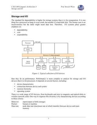
  • 1. C SCI 360 Computer Architecture 3 Prof. Stewart Weiss Storage and I/O Storage and I/O The standard for dependability is higher for storage systems than it is for computation. It is one thing for a processor to hang or even crash, but another if a hard disk fails. The former case is an inconvenience but the latter might mean data loss. Therefore, I/O systems place greater emphasis on: • dependability • cost • expandability than they do on performance. Performance is more complex to analyze for storage and I/O devices than it is for processors. It depends on several factors, including: • device characteristics • connection between device and system • memory hierarchy • operating system There is a wide range of I/O devices, from keyboards and mice to magnetic and optical disks to wireless network cards. One way to organize this diversity is by characterizing devices according to three criteria: Behavior: input/output or both (storage) Partner: human or machine Data rate: peak data rate (maximum rate at which transfers between device and main memory 1 Figure 1: Typical collection of I/O devices
  • 2. C SCI 360 Computer Architecture 3 Prof. Stewart Weiss Storage and I/O Assessing Performance Should performance be measured by • system throughput (jobs completed per unit time), or • response time? Throughput can be measured by bandwidth, either (1) number of completed I/O operations per unit time, or (2) number of bytes transferred per unit time Examples. 1. Transaction processing systems such as on-line commerce applications and on-line banking systems have to handle a large number of small transactions, so (1) is a better measure than (2). 2. A system for delivering streaming video, on the other hand, is better measured by the volume of bytes transferred per unit time (2) than by the number of completed transactions. Throughput is not always the best measure. Sometimes response time is more important. Often not just the mean response time, but the standard deviation of response times (indicates how reliable the system is). For single-user workstations, response time is typically the most important performance measure. Sometimes both are equally important: 3. ATM networks, file servers, and web servers must have short response times for their customers and must also process large amounts of data quickly. Dependability, Reliability, and Availability Dependability is the quality of a system such that reliance can be placed on its service. The service delivered by a system is its observed actual behavior as perceived by another system that interacts with it. The other system may be a machine, a person, or both. Dependability is therefore dependent on a reference point, since it may be different to different observers. To remove this subjectivity, there needs to be a reference standard, called a system specification, that specifies expected behavior. When such a specification exists, one can define: 1. Service accomplishment -- the state during which service is being delivered (meets specification). 2. Service interruption -- the state in which the delivered service is different from the specified service. This could mean no service at all, or service that fails to meet the specification. A failure is a transition from state 1 to state 2. A transition from state 2 to state 1 is called a restoration. 2
  • 3. C SCI 360 Computer Architecture 3 Prof. Stewart Weiss Storage and I/O Failures can be permanent or intermittent. Intermittent failures are harder to diagnose. Reliability is a measure of continuous service accomplishment. Equivalently, it can be measured by the mean time to failure (MTTF). (The amount of time it is available without interruption, on average.) Annual failure rate (AFR) is related -- it is the average number of failures per year, i.e., the average number of devices, that would fail in a year for a given MTTF. Service interruption is measured by how long a system is unavailable, which is characterized by the mean time to repair (MTTR). Mean time between failures (MTBF) is the sum of MTTF and MTTR. You can think of it as the time to the next failure plus the time it takes to repair that failure and bring the system back to the available state. This sum is the time from the last time it was brought up to the next time it was brought up. Availability is defined as Availability = MTTF/ (MTTF + MTTR) Then 0 <= Availability <= 1.0. It is the fraction of time that a system is achieving service accomplishment. To improve MTTF, either one improves the quality of the components or makes the entire system more fault tolerant. A system is fault tolerant if a failure does not lead to unavailability. A fault is a failure of a component. Hence MTTF can be improved by either: 1. Fault avoidance -- make the components better do that they do not fail as frequently. 2. Fault tolerance -- use redundancy to allow service to continue to meet the specification despite the occurrence of faults. RAID is an example of building fault tolerance into a storage system. 3. Fault forecasting -- predicting the presence and creation of faults, both hardware and software, to allow for replacing it before the failure occurs. 3 Figure 2: Summary of studies of causes of failure, from Ptterson/Hennessey
  • 4. C SCI 360 Computer Architecture 3 Prof. Stewart Weiss Storage and I/O Disk Storage Magnetic Disks All magnetic disks have the following properties in common: • One or more rotating platters (they rotate in unison) • Magnetic coated surface • Movable read/write head • Nonvolatile • Rotation speed from 5400 to 15000 RPM There is some important terminology to remember regarding the structure of a magnetic disk drive: • A platter is one disk of a set of one or more coaxial disks. • A surface is one of the two surfaces of any platter. Each surface is divided into a set of concentric circles, called tracks. • A track is one of the concentric rings on a surface on which the data is recorded. • A sector is the consecutive sequence of bits on a track within a pre-specified arc of the circle. • A cylinder is the set of all tracks under the read/write heads, on all surfaces, at a given time Tracks are not necessarily divided into the same number of sectors. Inner tracks may have fewer sectors than outer tracks. The idea is to keep the bits uniformly spaced in each track. This is called zone bit recording (ZBR). Performance Costs To perform a read or a write on a disk, three steps must be taken: 1. The read/write heads must be moved in or out until they are positioned over the appropriate track. This is called seeking. 2. The head then waits until the right sector has moved under the head. 3. The data is transferred to or from the disk. Each of these steps has an associated cost in terms of time: • Seek time The amount of time for the heads to move to the right track • Rotational latency The time spent waiting for the right sector to rotate under the heads. (Also called rotational delay.) • Transfer time The time to transfer a block of bits, which depends upon sector size, rotation speed, and the recording density of the track. 4
  • 5. C SCI 360 Computer Architecture 3 Prof. Stewart Weiss Storage and I/O In addition, there is a fourth component to the overall time overhead that is related to the disk controller. The disk controller is the disk's processing unit and is responsible for receiving instructions and data and controlling the activities of the disk. The controller's execution time is another factor in the overhead of disk I/O: • Controller overhead The time spent by controller to initiate and finalize I/O transfers. The complication in true performance estimation is that modern controllers come with very large caches and do anticipatory caching of sectors. Transfer time from the cache to the processor is much smaller because there is no mechanical operation involved; the data are read from or written to the cache directly. Common Measures Disk manufacturers usually report minimum seek time, maximum seek time, and average seek time. Average seek time depends upon many factors and so is not always useful. Typical average seek times are between 3 ms and 13 ms. Average rotational latency is between ½ rotation / minimum rotations per sec = 0.5 /5400 RPM = 0.5/90 sec = 0.0056 sec = 5.6 ms and ½ rotation / maximum rotations per sec = 0.5 /15000 RPM = 0.5/250 sec = 0.002 sec = 2.0 ms Transfer time depends on sector size, recording density, and rotation speed. Typical transfer rates are between 125 MB/sec and 200 MB/sec, but when transfers are measured from the cache, they can be as much as 400 MB/sec. Example What is the average time to read or write a 512 byte sector for a disk rotating at 5400 RPM, given advertised • average seek time = 12 ms • transfer rate = 5 MB/sec • controller overhead = 2 ms Time to read a 512 byte sector is = seek time + rotational latency + transfer time + controller overhead = 12 ms + 0.5/(5400/60) sec + 512 bytes/(5 MB/sec) + 2 ms = 12 ms + 5.6 ms + 0.1 ms + 2 ms = 19.7 ms 5
  • 6. C SCI 360 Computer Architecture 3 Prof. Stewart Weiss Storage and I/O Rotational delay can be the dominating cost if seek time is much less. Flash Storage Flash memory is a type of EEPROM (electrically erasable programmable read-only memory) that has grown in popularity because: • it is durable (resistant to shock) • it is compact • it is power-efficient • it has much smaller latency than hard disks In addition, its capacity is usually large enough for many applications (cameras, phones, media players) but is available in small capacities for small devices. Because of these features, it is the first technology that is competitive with magnetic disks in the secondary storage market. There are two types of flash memory: NOR flash and NAND flash. The original technology was NOR flash. NOR flash provided random access memory. NAND flash provided much more storage capacity but could only read and written in blocks. In addition it is much less expensive than NOR flash. Characteristics NOR flash NAND flash Typical use BIOS USB key Minimum access size (bytes) 512 2048 Read time (msec) 0.08 25 Write time (msec) 10.00 1500 to erase + 250 Read bandwidth (MB/sec) 10 40 Write bandwidth (MB/sec) 0.4 8 Wear-out (writes per cell) 100,000 10,000 to 100,000 Best price/GB (2008) $65 $4 Table 1: NOR versus NAND flash memory comparison (from Paterson & Hennessey). The limiting factor is that bits wear out with writes over time. The table above shows that NAND flash will wear out faster than NOR flash. Flash drive controllers reduce the chance of wear-outs by trying to distribute writes uniformly across the memory. They do this by moving logical blocks that have been written a lot to different physical blocks. This is called level wearing. 6
  • 7. C SCI 360 Computer Architecture 3 Prof. Stewart Weiss Storage and I/O Connecting Processors, Memory, and I/O Devices A bus is a shared communication path whose purpose is to allow the transfer of data among the devices connected to it. A bus includes address, control, and data lines as well as lines needed to support interrupts and bus arbitration. Control lines include a read/write line. A bus protocol is a set of rules that govern the behavior of the bus. Devices connected to the bus have to use these rules to transfer data. The rules specify when to place data on the bus, when to assert and de-assert control signals, and so on. Among methods of interconnecting components of a computer system, buses are • versatile • low-cost • a major bottleneck Bus speed is limited by: • bus length • number of attached devices Buses can be synchronous or asynchronous; synchronous buses use a clock to control transfers, whereas asynchronous buses do not. This is discussed further below. Because of clock skew and signal reflection, it is difficult to design buses with many parallel wires at high speed. Clock skew is the difference in absolute time between when two state elements see a clock edge. Clock skew arises because the clock signal will often use two different paths, with slightly different delays, to reach two different state elements. When the length of the wires is long and clock speeds are fast, skew can become a problem. The reflection of the clock signal is also a problem as clock speeds get faster. Buses are gradually being replaced by serial point-to-point interconnection networks with switches. Nonetheless, we begin with a brief overview of buses. Bus Types Different kinds of buses are used to connect different parts of a computer system to each other. Processor-Memory Bus These are sometimes called processor buses. They are short, high speed buses, usually designed for a specific memory and processor to maximize bandwidth. They can be used when all devices that can be attached are known in advance and have known characteristics. Typically these are proprietary buses. I/O Bus I/O buses have varying length and usually allow many different kinds of devices with varying speeds and data block sizes to be attached. I/O buses may be connected to the processor bus via a 7
  • 8. C SCI 360 Computer Architecture 3 Prof. Stewart Weiss Storage and I/O bridge or a separate controller interface, but usually they are connected to what is often called a system, or backplane, bus, described below. I/O buses are almost always standard, off-the- shelf components. Examples include SCSI, USB, PCI Express, Serial ATA (SATA), and Serial attached SCSI (SAS) . Backplane, or System, Bus Most modern computers use a single, general-purpose bus to interconnect a variety of internal devices, including network interface cards, DMA controllers, and hard disk drives. These buses used to be called backplane buses but are now often called system buses. Usually, I/O buses are connected to the system bus, which in turn connects to the processor bus via a bridge. Connection Basics In any transfer operation, there are two parts -- sending the address and sending or receiving data. The device initiating the request is called the master, and the one receiving the request is called the slave. The processor is often the master, but memories can be masters as well. When it comes to buses, the direction of the operation is defined from the perspective of memory: A read operation is one that transfers data from memory to a device, and a write operation transfers data from a device into memory. To clarify the language, we can avoid using read and write and instead use input and output. Input refers to transfers from devices into memory, and output refers to transfers from memory to devices. Synchronous Buses A synchronous bus has a clock line accessible to all attached devices, and a clock that generates uniform pulses on the line. A bus cycle is the interval between one or more consecutive pulses. The simplest synchronous bus uses a single long clock cycle for data transfers and ensures that all data transfers take one clock cycle. The cycle is long enough to accommodate all devices. This design is inefficient because all transfers take as long as the slowest device. Sometimes instead of a single cycle, all transfers take a fixed number of cycles greater than 1. More general synchronous buses use a higher frequency clock rate and allow different devices to use different numbers of clock cycles for a single transfer. One device might respond after two clock cycles and another might require five. In all synchronous buses, the bus protocol is based upon the use of clock cycles exclusively to coordinate transfers of data. Example A simplistic (and unrealistic) protocol to input a word from memory to the processor : transmit a read request on the R/W control line and address on data line wait 5 clock cycles; store data from memory into processor location 8
  • 9. C SCI 360 Computer Architecture 3 Prof. Stewart Weiss Storage and I/O Advantages • Relatively simple control logic • Usually fast, because the protocol uses little bus overhead Disadvantages: • Does not work if bus length is too great because clock skew (clock signals arriving at different times from different devices) can corrupt logic. • Must be designed to accommodate the slowest device. • Adding new devices complicates the design. Asynchronous Buses Most of the popular buses in use in 2011 are asynchronous, including USB 2.0, PCI Express (PCIe), Serial ATA (SATA), Serial Attached SCSI (SAS) and Firewire. An asynchronous bus is not clocked. Instead, devices communicate by exchanges messages with each other. These messages are called handshakes. Because it is not clocked, it is a more versatile bus, but the complex, handshaking protocol can consume more overhead. Handshaking is like the please-and-thank-you protocol that people use in everyday life. Each party in a communication expects a certain response to its message and until it receives that response, it does not advance to its next logical state. Think about a telephone call. When you call, you expect the person responding to answer with some verbal message such as “hello” or 9 Figure 3: Traditional I/O Interconnections and Buses Processor Memory Bridge ProcessorBus PCIBus(systembus) SCSI Controller Ethernet Interface USB Controller SCSIbus SCSIDisk Controller Printer Joystick CD-ROM Controller
  • 10. C SCI 360 Computer Architecture 3 Prof. Stewart Weiss Storage and I/O “this is so-and-so.” That person expects you to reply with a greeting in return, and if no reply is forthcoming, he or she will hang up. Advantages • Handshake eliminates need for synchronization of clocks • Can be unlimited length • Can add devices or change delays without redesign of bus • Can support a wide variety of devices Disadvantages • Generally slower than synchronous buses for short lengths The I/O Interconnects of the x86 Processors The I/O system depicted in Figure 4 is typical of that of all x86 processors. There are two controller hubs, called the north bridge and the south bridge. The processor connects to memory and peripheral devices via these hubs. The north bridge is the memory controller hub, and connects the processor to the memory, the south bridge, and sometimes the graphics card (via a PCIe bus.) The south bridge is the I/O controller hub and connects the processor to all I/O devices, through a number of different kinds of attached buses such as the USB, PCI, SATA and so on. 10 Figure 4: Schematic organization of the Intel 5000P I/O system (from [Paterson/Hennessey])
  • 11. C SCI 360 Computer Architecture 3 Prof. Stewart Weiss Storage and I/O Some processors, such as the AMD Opteron X4, incorporate the north bridge into the processor ship instead of its being a separate chip. Interfacing I/O Devices to the Processor, Memory, and OS This section answers the following questions: • How is an I/O request transformed into device-specific commands? • How is an I/O request actually communicated to the I/O device? • How is data transferred to or from the memory? • What are the respective roles of the application level software, the operating system, and the hardware? The answers to these questions will vary depending upon how the computer system is designed to be used. Most modern computers and operating systems support multi-processing, interactive use, and multiple users. To provide these features, the operating system must perform under the following constraints: • The I/O system is shared among multiple processes. • If processes are allowed to control devices directly, then throughput and response time will not be under the control of the operating system, and the computer system will perform poorly. • If user processes are required to issue I/O requests directly to devices, then the programming task becomes much more tedious for the software engineer. • I/O requests should be handled by the operating system, and the operating system must determine when the requested I/O has completed. • Because I/O is handled by the operating system, the operating system must provide equitable access to I/O resources and device abstraction. To satisfy these constraints, the operating system must be able to communicate with devices and prevent user programs from communicating with these devices. There are three differernt types of communication: • Issuing commands to devices (e.g., read, write, seek, start, stop) • Receiving notifications when devices need attention (e.g., I/O completion, error, load media) • Transferring data between memory and a device. The most common paradigm used in operating systems is a multi-layered approach to resources. Users make requests for I/O to application software. Application software translates these requests into calls to the operating system. The device drivers are the operating system’s lowest level software; they are really two parts. One part issues I/O commands to the devices. The other part responds to signals sent by the device to the processor when they need attention. Together they maintain the queues needed to coordinate the requests. The operating system notifies applications when the I/O is completed. 11
  • 12. C SCI 360 Computer Architecture 3 Prof. Stewart Weiss Storage and I/O Giving Commands to I/O Devices In order for the processor to issue a command to an I/O device, it has to be able to address the device and it has to be able to deliver one or more commands to it. There are two different methods of addressing devices: memory-mapped I/O and special I/O instructions. Memory-Mapped I/O In memory-mapped I/O, parts of the address space are reserved for I/O device ports. Device port locations are mapped to specific memory addresses in such a way that when the processor accesses these locations, it is really accessing the device ports. Ordinary instructions are written to these addresses in order to perform I/O as if they were data. When the processor references an address in this special part of the address space, the memory controller ignores the address; instead the hardware translates this to the corresponding I/O device register. The I/O device controller receives the data and interprets it as a command which it can then carry out. Certain addresses are used for specific commands. For example, one address might be for reads from the device and another, for writes. In the Intel IA-32 instruction set, the identifiers DATAIN and DATAOUT are mnemonic names for memory addresses that are mapped to I/O device registers. The ordinary MOV machine instruction MOV AL, DATAIN moves a character from the device register into register AL and the instruction MOV DATAOUT,AL moves a character from register AL to the device register. An example of an IA-32 I/O program to read from the keyboard and echo the characters on the screen is shown below. IA-32 is a 32- bit Intel instruction format. Example (Intel IA-32 instructions) In the Intel-32 instruction set, there are two device status registers, INSTATUS and OUTSTATUS. The following program assumes that the keyboard synchronization flag is stored in bit 3 of INSTATUS and the display synchronization flag is stored in bit 3 of OUTSTATUS. LEA EBP,LOC # Register EBP points to LOC, the memory area READ: BT INSTATUS,3 # INSTATUS bit 3 is set if there is data in JNC READ # DATAIN; this loops waits for data MOV AL,DATAIN # Transfer char into register AL MOV [EBP],AL # Transfer AL contents to address in EBP INC EBP # and increment EBP pointer ECHO: BT OUTSTATUS,3 # Wait for display to be ready JNC ECHO MOV DATAOUT,AL # Send char to display CMP AL,CR # If not carriage return, JNE READ # read more chars Notes. • LEA reg, addr is an instruction to load the address addr into the pointer register reg. 12
  • 13. C SCI 360 Computer Architecture 3 Prof. Stewart Weiss Storage and I/O • BT is a bit-test instruction. It loads the value in bit 3 of the specified register into the carry bit; JNC will branch if the carry bit is 0. Figure 5 illustrates the basic structure of the connections when memory-mapped I/O is used. The four bus lines are for data, addresses, a read signal, and a write signal. Figure 6, in contrast, shows the structure when special I/O instructions are used. In this case there are separate control lines from the CPU to memory and from the CPU to the I/O devices. Figure 5: Lines used in memory-mapped I/O Communicating Via Special I/O Instructions In isolated I/O, or I/O-mapped I/O, the processor has special instructions that perform I/O and a separate address space for the I/O devices. In isolated I/O, the same address lines are used to address memory and the I/O devices; the processor asserts a control line to indicate that the I/O devices should read the address lines. All I/O devices read the address but only one responds. For example, in the IA-32 instruction format, IN REGISTER,DEVICE_ADDR and OUT DEVICE_ADDR,REGISTER are the input and output instructions respectively. DEVICE_ADDR is an 8-bit address, and REGISTER is either AL or EAX. Some instruction sets, such as the IA-32, support both memory-mapped and isolated I/O. In Figure 6 the separate physical lines for communicating with the I/O devices and memory are labeled READIO and WRITEIO to symbolize that special commands would be issued to use these lines. 13 I/O DeviceB I/ODeviceA Memory I/OPort 1 I/OPort 2 I/OPort 3 CPU
  • 14. C SCI 360 Computer Architecture 3 Prof. Stewart Weiss Storage and I/O Figure 6: Isolated I/O (using special I/O instructions) Methods of Controlling I/O There are three basic methods of controlling I/O and interacting with devices: polling, interrupt- driven I/O, and direct memory access (DMA). These are described in turn. Polling (Program-controlled I/O) The program above that reads from the keyboard and echos the characters to the screen is an example of polling. In polling, every byte of data is transferred under the control of the CPU. An I/O program issues instructions to the I/O device to transfer the data. The data is transferred to or from memory by the program. On a read, for example, the program must request the input operation and then repeatedly test the status of a bit or register to see if the input is available. It does this in a “busy-waiting” loop in which it “polls” the device to see if it is ready. In effect, it is the nagging child on the long trip, “are we there yet, are we there yet, are we there yet,…” until at long last we have arrived. This method is appropriate if the performance requirements are not great and the hardware does not support the other methods. In general, it is wasteful of computing cycles. In certain situations, polling is a good solution, such as when I/O rates are completely predetermined. In this case, the processor knows exactly when the data will be ready, so the overhead is predictable. The disadvantage of polling is that the processor is completely consumed with the I/O, spinning in idle cycles waiting for the I/O device to finish, which is a waste of valuable CPU cycles, especially if the frequency of polling is great. The following example demonstrates this. Example. Assume that a computer has a 500 MHz clock, and that the instructions in the operating system that are executed to perform the polling operation use 400 clock cycles. What is the overhead to poll each of the following three devices, with the stated characteristics? 1. Mouse: can produce an event 30 times per second. 14 Memory I/O DeviceB DATA ADDR WRITE WRITEIO I/ODeviceA I/OPort 1 I/OPort 2 I/OPort 3 READIO CPU READ
  • 15. C SCI 360 Computer Architecture 3 Prof. Stewart Weiss Storage and I/O 2. Floppy disk: can transfer 2-byte blocks at a rate of 50KB/second. 3. Hard disk: can transfer 4-word blocks at a rate of 4MB/second. Solution. The operating system uses 400 2ns clock cycles per polling operation, or 800 ns. Mouse: 30*800 ns /second = 0.000024 or 0.0024%. Floppy Disk: 50KBytes/sec at 2 bytes per transfer implies that it performs 25,000 transfers per second. The overhead is 25,000*800 ns/second = 0.02 or 2%. Hard Disk: 4MB/second at 4 words per transfer implies that it transfers 250,000 times per second. The overhead is 250,000*800 ns/ second = 0.2 or 20%. This shows that the faster the device, the more overhead is involved in polling as a means of controlling I/O. Interrupt-driven I/O An alternative to programmed I/O is In interrupt-driven I/O. In interrupt-driven I/O, a program running on the processor issues an I/O command to a device and then goes into a waiting state. Another process is run on the processor while the I/O is carried out. When the I/O completes, the I/O device sends a signal, called an interrupt, to the processor. This signal is like an exception except that it is asynchronous. This requires adding more signals to the bus and more logic to the I/O devices to allow them to notify the CPU when the device is ready for a new I/O operation, or when an I/O operation is complete. There are various ways to arrange this, some more complex and flexible than others. Regardless of the method, it has to provide a means of deciding which device caused the interrupt. Figure 7: Interrupts with a single interrupt request line The simplest scheme is a single control line on the bus, usually denoted INTR. All devices share this line. The line is the logical OR of the interrupt requests of the attached devices. If any device has issued an interrupt, the processor receives the signal. The processor then has to determine 15 CPU Interrupt Flip-Flop Device1 Device2 Device3 InterruptRequestLineINTR INTA
  • 16. C SCI 360 Computer Architecture 3 Prof. Stewart Weiss Storage and I/O which device issued the request, which it does by polling the status registers of the devices. Once it has determined which device issued the request, it can initiate the transfer of data. If interrupts arrive at the same time, the processor has to decide which to accept. Generally, it does this by assigning priorities to the devices. With a single interrupt line, priorities can be assigned by using a daisy chain scheme like the kind used for bus arbitration. In a daisy chain, the devices are arranged in a sequence such that each device is connected to the next one and passes messages down the line if they are not addressed to it. That is the purpose of the INTA line in Figure 7, which runs through the devices. The processor sends an Interrupt Acknowledge signal through the line. The closest device that has an outstanding interrupt request intercepts the signal. Another solution is to use a multiple-line interrupt system. In this case each device has a dedicated INTR line and a dedicated INTA line. This makes it easy to decide which device caused the interrupt. The lines run into a priority arbitration circuit in the CPU. The CPU chooses the highest priority interrupt. Handling Interrupts When an interrupt occurs, the CPU needs to execute the subroutine that handles, or services, the interrupt. To do this, the contents of some of its registers must be saved. Modern processors typically allow two types of interrupts, one that forces a save of the entire register set, and another that saves only a minimal set of registers. The latter is the more efficient solution since only a few registers are saved, and the subroutine can choose to save whatever other registers it needs to in order to execute. This is faster than saving all registers, and avoids unnecessary work if there is no need to save them. The registers may be saved in special dedicated storage, or put on the system stack. The interrupt service routine (ISR) runs, saves whatever CPU state it must, and on completion, either the previous instruction sequence is resumed, or the scheduler is run to pick a different process to run. How does the operating system know which ISR to execute? The answer is that once it knows which device caused the interrupt it knows which subroutine to run. In vectored interrupts, there is a portion of memory that contains an array, i.e., a vector, each of whose cells is the starting address of an interrupt service routine (ISR). Each device has an entry in this vector. When an interrupt occurs, the address of the device is used as an index into this array, and the starting address of the interrupt service routine is automatically loaded, once the registers have been saved. There are other issues related to interrupts. They include: 1. Should interrupts be disabled while an interrupt service routine is running? If so, is the interrupt lost, or is it just that the response is delayed? 2. If not disabled, what happens if an interrupt occurs while an interrupt service routine is running? There are various answers to these questions, depending on the complexity of the system. There are usually two registers, a Cause Register and a Status Register, used to solve the first 16
  • 17. C SCI 360 Computer Architecture 3 Prof. Stewart Weiss Storage and I/O question. The Cause Register has a bit for each different interrupt. If an interrupt occurs, the bit is set to 1, otherwise it is 0. The Status Register bits are used as an interrupt mask. If an interrupt is enabled, there must be a 1-bit in the corresponding position in the Status Register. AND-ing the two registers gives the set of enabled interrupts that have occurred. The mask can be used to set the interrupt priority level of the processor by a left-to-right ordering of the mask bits. If an interrupt occurs whose bit is to the left of another one, it has higher priority. By turning off all bits to the right of a given bit, the processor masks all lower level interrupts than a given level. If an interrupt occurs that is lower priority than the current priority level, it is ignored. If one occurs that is a higher or equal priority, the currently running process is preempted in favor of the interrupt service routine that handles the new interrupt, regardless of what it was doing. Each device has an associated priority level, and the ISR for that device runs at that priority level. For example, the power supply can send an interrupt if it senses an impending loss of power. This is the highest priority level on many machines. The system timer is also very high priority; it must keep accurate time and uses very little CPU time when it runs, so it is reasonable to allow it to run whenever it needs to, which is on the order of 60 times per second. Overhead The overhead of interrupts is much lower than that of program-controlled I/O. To illustrate, consider the hard disk from the preceding example, which could transfer 4-word blocks at a rate of 4 MB/second. Suppose that the operating system needs 500 clock cycles of processing time to handle an interrupt and that the disk is only busy 5% of the time. For each of the 250,000 transfers per second that the disk generates, the interrupt service routine, uses 500 clocks * 2 ns/clock = 1000 ns. Since it is busy 5% of the time, the overhead is 5% of 250,000 transfers * 1000 ns per transfer per second = 0.05 * 250,000,000 ns per second = 12,500,000 ns/second , which is 1.25%. Recall that polling used 20% of the CPU time, so this is 93.75% reduction in overhead (1.25/20 = 0.0625, so 1.25% is 6.25% of 20%.) 17
  • 18. C SCI 360 Computer Architecture 3 Prof. Stewart Weiss Storage and I/O Direct Memory Access (DMA) Direct Memory Access (DMA) is a method of transferring data at a very high bandwidth with low overhead. The processor, under program control, effectively authorizes the a special device to take charge of the I/O transfers to memory, allowing it to be the bus master until the I/O is completed. A device with this capability is called a DMA controller. Figure 8: Circuitry for DMA interface DMA significantly reduces the involvement of the processor in data transfers between memory and I/O devices. A DMA controller is an I/O processor that has the ability to communicate directly with memory, transferring large blocks of data between memory and the I/O devices to which it is attached. It achieves this because it is attached to the processor-memory bus on one side, and either an I/O bus or a dedicated device on the other, and it can be bus master on the memory bus. Typically, a single DMA controller will service multiple I/O devices. Certain devices, usually high-speed devices such as hard disks, CD-ROM drives, or network interfaces, may be equipped with DMA controllers. For example, a SCSI bus controller will have a DMA controller in its interface, making it possible for all devices on the SCSI bus to transfer data directly to or from memory with little CPU involvement. A program running on the CPU will give the DMA controller a memory address, the number of bytes to transfer, and a flag indicating whether it is a read or a write. It will also give it the address of the I/O device involved in the I/O. The DMA controller becomes the bus master on the memory bus. If it is an input operation, the device will then start sending data to the DMA 18 Main Memory IOAR I/O Address Register Data Counter IODR I/OData Register Control Unit DMA Controller Address Register Register File Control UnitCPU DMAAcknowledge Data Address Control DMARequest System Bus I/O Devices
  • 19. C SCI 360 Computer Architecture 3 Prof. Stewart Weiss Storage and I/O controller, which will buffer the data, and store it in successive memory locations as it becomes available. If it is an output operation, it buffers the data from memory and sends it to the I/O device as it becomes ready to receive it. In effect, it does what the CPU would do, but the CPU is free to do other things in the meanwhile. Figure 8 depicts the circuitry in a typical DMA controller interface. The typical sequence of operations in an input transfer would be: 1. The CPU executes two instructions to load the IOAR and the Data Counter. The IOAR gets the start address in memory of the first byte to be stored and the Data Counter gets a count of the number of bytes to be transferred. 2. When the DMA controller is ready, it activates the DMA request signal. 3. The CPU relinquishes control of the bus and activates DMA Acknowledge as part of the handshake. 4. The DMA controller begins the transfer of data to memory using a hardware loop to update the IOAR and Data Counter. 5. If the I/O device is not ready, but the transfer is not complete, the DMA controller relinquishes the bus so that the processor can use it. 6. If the I/O device was not ready and it becomes ready, the DMA controller re-acquires the bus in the same way it did in above. 7. When the Data Counter reaches 0, the DMA controller releases the bus and sends an interrupt to the CPU. Because the DMA controller owns the bus during a transfer, the CPU will not be able to access memory. If the CPU or the cache controller needs to access memory, it will be delayed. For small data transfers this may be acceptable, but not for large transfers, because it defeats the purpose of using DMA in the first place. Therefore, DMA controllers usually operate in two modes, one for small transfers and one for larger transfers, in which "cycle-stealing" is allowed. In cycle-stealing, the CPU is allowed to interrupt the DMA transfer and acquire the bus. DMA Overhead Example Suppose that a system uses DMA for its hard disk. The system characteristics are: 1. System Clock: 500 MHz (2 ns per cycle) 2. Hard Disk can transfer at 4MB/second using an 8KB block size. 3. 1000 clock cycles are used in the CPU to setup the I/O and 500 clock cycles are used afterwards in the CPU. What is the overhead of DMA transfers? Each transfer takes 8KB / ( 4MB/ second) = 0.002 seconds (2 ms). Thus there are 1.0 / 0.002 = 500 transfers per second. If the disk is busy then it takes (1000 + 500) * 2 ns per transfer, which is 3000 ns per transfer. Since there are 500 transfers per second, the total overhead is 500*3000 ns per second, or 1.5 ms per second, which is 0.15%. 19
  • 20. C SCI 360 Computer Architecture 3 Prof. Stewart Weiss Storage and I/O DMA and Virtual Memory In a system with virtual memory, DMA poses a problem – should the DMA controller use virtual or physical addresses? If it uses physical addresses, then it cannot perform reads or writes that cross page boundaries. To see this, imagine that pages are each 1 KB. If the DMA controller tries to write 3KB of data, then it will write into 3 or 4 physical pages. These pages may not belong to the same process, and may not be logically adjacent, and should be placed in the logically correct memory locations. On the other hand, if it uses virtual addresses, it will need to translate every address, slowing things down considerably and requiring a large RAM of its own. One solution is for the DMA controller to keep a cache of translations in its memory and update it using a replacement strategy such as LRU. This is still inadequate because the page translations it has may go stale if the processor updates the page tables independently. For DMA to work properly, the processor must be prevented from changing the page tables during a DMA transfer. DMA and Cache DMA also creates problems with the cache. If the DMA controller is reading data directly from the disk into memory, then cache blocks may become stale, because the cache blocks will not be consistent with their corresponding memory blocks, which are newer. This is called the stale data problem. Similarly, the DMA controller might read from memory and get stale data because the system has a write-update cache that has not yet been flushed to memory. There are a few solutions: • Route all I/O through the cache. • Flush the cache for I/O writes and invalidate it for I/O reads. To make this efficient, special hardware is provided for flushing the cache. I/O Performance Measures Remember that I/O performance can be measured by throughput or response time or a combination of both. Which we choose depends upon how the system will be used. Over time, computer scientists have developed collections of programs called benchmarks that are run on systems to measure their performance. The benchmarks are designed for specific purposes, such as to measure the performance of a transaction processing system, or a supercomputer, or a web server, and so on. These benchmarks have specific characteristics, which are summarized below. Before continuing, remember that I/O transfer rates are measured in decimal units, not binary units: 1 MB = 10^6 bytes, not 2^20 bytes. Supercomputer I/O Benchmarks Supercomputer benchmarks are characterized by two factors: • They are dominated by file accesses; typically output is much greater than input. • I/O throughput is more important than response time or latency. 20
  • 21. C SCI 360 Computer Architecture 3 Prof. Stewart Weiss Storage and I/O Transaction Processing I/O Benchmarks Transaction processing systems have both response time and throughput requirements. Throughput is usually measured by the I/O rate, which is the number of completed I/O accesses per second, since the amount of data per transaction is small. Since the data rate (bytes per second) is small, it is not a good measure of performance. Response time is the amount of time between when the transaction is received and the database is accessed and possibly modified. Benchmarks are therefore characterized by • Small, frequent I/O accesses • Response time requirements • Variable profile of transactions to simulate different types of applications (business versus web server or application server, for example) File System and Web I/O Benchmarks File system I/O performance depends on the sizes of files and the types of accesses. For example, SPECSFS97 was a popular benchmark designed for NFS (a UNIX file system) that measured file system and network I/O throughput with response time constraints. It is no longer in use. Web server I/O performance depends on the type of web accesses, i.e., uploads versus downloads, static versus dynamic pages, page sizes, and so on. SPECWeb2009 is a benchmark that simulates a mix of clients. The Downside of Benchmarks A drawback in the use of benchmarks to assess computer systems is that, once a particular set of benchmarks has entrenched itself in the minds of the customers who are interested in purchasing machines, the hardware manufacturers start to design their machines so that they perform well on the benchmarks. Is this a bad thing? Yes, it certainly is. A benchmark is an approximation of the "average" user's workload on the machine. No matter how it is configured, it is simply a model of the imaginary typical customer that the benchmark's designers fashioned. It is an abstraction. While benchmarks can be configured and customized, those changes are within the set of constraints imposed on it by its design. For example, SPECWeb2009 does not model latency associated with obtaining data across a wide-area network such as the Internet. A benchmark can end up rewarding bad engineering decisions because of its design, if it puts more weight on little used operations than it should or it if fails to take into considerations important factors. Therefore, it is best not to rely too heavily on the results of benchmark tests. Example of Impact of I/O on System Performance A benchmark program executes in 100 seconds of elapsed time in which 90% of the time is spent in the CPU and 10% is in waiting for I/O. Suppose that the number of processors doubles every two years, but they remain the same speed, and the I/O time does not change. How much faster will the program run at the end of six years? 21
  • 22. C SCI 360 Computer Architecture 3 Prof. Stewart Weiss Storage and I/O Elapsed time is CPU time plus I/O time. The CPU time is divided by the number of processors, but the I/O time remains the same. The following table illustrates the changes in elapsed time and CPU time over the 6-year period of the problem. Years elapsed CPU Time (seconds) I/O Time Elapsed Time % I/O Time 0 90 10 100 10 2 90/2 = 45 10 55 18 4 45/2 = 22.5 10 32.5 31 6 22.5/2 = 11.25 10 21.25 48 After six years, the elapsed time is 11 seconds; the speed increase is 100/21.25 = 4.7 (470%) even though there are 8 times as many processors. The theoretical improvement, had I/O kept pace with CPU improvements would be 800%. Redundant Arrays of Inexpensive Disks (RAID) RAID was originally invented to improve I/O performance. The idea was to replace a few large disks by many smaller disks. This would result in more read heads, fewer seeks, more independent simultaneous accesses, reduced power consumption, and smaller space requirements. It was also believed that smaller disks were less reliable, so to compensate, redundancy was added in the form of additional disks. The result was RAID. RAID is now used primarily as a means of increasing reliability and dependability, not performance. Summary of RAID RAID is categorized by the RAID level, an integer from 0 to 6. The different levels differ by how much redundancy there is and how errors are checked. RAID 1 and RAID 5 are the most widely used. The following is a brief synopsis. RAID 0 - There is no redundancy; it is designed to improve performance by the use of striping. Striping is the distribution of consecutive blocks of data across multiple disks (in the same of nearby cylinders). RAID 1 - Uses mirroring, which is a technique in which the disks are doubled and each write is replicated on a second disk. RAID 2 - Uses error detecting and correcting code; it is not in use, having been replaced by higher levels. RAID 3 - Uses bit-interleaved parity; improves on RAID 1 by adding only enough redundant data to the secondary disks to be able to restore the lost data on the primary. Parity is a simple example of RAID 3 -- for a group of N disks there will be an extra disk, which stores the sum of 22
  • 23. C SCI 360 Computer Architecture 3 Prof. Stewart Weiss Storage and I/O the data from those disks. If a disk fails, it can be reconstructed by adding the other disks and subtracting from the parity disk. If two go bad, this fails. RAID 4 - Uses block-interleaved parity; this is similar to RAID 3, but it uses a different method of parity checking. RAID 5 - Uses a distributed block-interleaved parity, which is an enhancement of RAID 4. The problem with RAID 4 is that the parity disk must be updated on every write. In RAID 5, the parity information is distributed across all of the disks. RAID 6 - Uses P+Q redundancy, which is a method of error correction that allows the disks to recover from two simultaneous failures. Alphabetical Index annual failure rate..........................................3 asynchronous bus..........................................9 availability.....................................................3 backplane bus................................................8 benchmarks.................................................20 bus.................................................................7 bus cycle........................................................8 bus protocol...................................................7 clock skew.....................................................7 controller overhead.......................................5 cylinder .........................................................4 daisy chain...................................................16 data rate.......................................................21 dependability.................................................2 Direct Memory Access................................18 DMA controller...........................................18 failure............................................................2 fault avoidance..............................................3 fault forecasting.............................................3 fault tolerance................................................3 flash memory.................................................6 handshakes....................................................9 I/O rate........................................................21 interrupt.......................................................15 interrupt service routine..............................16 interrupt-driven I/O.....................................15 level wearing.................................................6 mean time between failures...........................3 mean time to repair........................................3 memory-mapped I/O...................................12 platter............................................................4 polling.........................................................14 processor bus.................................................7 RAID...........................................................22 reliability.......................................................3 restoration......................................................2 rotational latency...........................................4 sector.............................................................4 seeking..........................................................4 service accomplishment................................2 service interruption........................................2 special I/O instructions................................12 stale data problem.......................................20 striping........................................................22 surface...........................................................4 synchronous bus............................................8 system specification......................................2 track...............................................................4 transfer time..................................................4 zone bit recording..........................................4 23