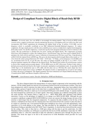
Design Efficient Wireless Monitoring Platform for Recycling Point Spots
Research Inventy: International Journal of Engineering and Science
1. RESEARCH INVENTY: International Journal of Engineering and Science
ISSN: 2278-4721, Vol. 1, Issue 9 (November 2012), PP 1-07
www.researchinventy.com
Design of Compliant Passive Digital Block of Read-Only RF ID
Tag
R. N. Baral1, Jagdeep Singh2
1,
Professor, EC E Deptt.
2,
M.TEC H. (VLSI) Final Year
1,2,
IMS Engg. College Ghaziabad (U.P) India
Abstract— In recent years, low cost RFID is increasingly becoming popular. Tags of such an RFID system
consists of less complex architecture, thereby minimizing the power consumption and cost will be less.The work
incorporates ISO 14443 regulations for designing the digital block of tag. It utilizes 13.56 MHz carr ier
frequency which is available worldwide as an ISM (Industrial -Scientific-Medical) frequency. To reduce
complexity, the tag is made passive with the only available power source as inductively coupled electromagnetic
field of the reader. For further simplicity, a read-only tag has been designed which just reveals its identity to the
reader. The tag architecture is divided into two parts: analog and digital blocks. The components of analog
block have been designed to reduce the leakage power. Asynchronous l ogic has been used in digital block to
minimize the clock activity and hence cause a reduction in transient power.We have used Type A specifications
of IS O 14443 for digital block of RFID tag. This gives the Interrogation field strength Hmin of the reader as 7.5
A/m. From the values of tag dimensions (85.72mm × 54.03 mm × 0.76mm), carrier frequency (13.56 MHz) and
no. of antenna turns (N=4), we get the min. rms value of voltage available to the tag U 2 as 2.581V. A Low
dropout regulator supplies the voltages for the digital block. The digital block utilizes an asynchronous counter
to derive their timing and processing signals. 128 bit ROM stores an EPC (Electronic Product Code) which is
fetched, processed and sent back to the reader via decoder, multiplexer a nd modulator units. As specified in ISO
14443 Type A, the modulation type is 10% ASK with the data rate as 106 kbps.The entire deign has been
simulated with an input power source of 600µW. The digital circuitry is implemented on 1V rail to rail voltage
to reduce the power consumption. The digital schematic has been simulated on 0.18µm CMOS technology Level
53 models from TSMC and Mentor Graphics EDA tool suite.
Keywords— Asynchronous counter, Decoder, Multiplexer, ROM and Modulator.
1. INTRODUCTION
The above diagram depicts the arrangements of various digital co mponents in the t ransponder with the
memo ry. A ll the timing signals are derived in asynchronous fashion fro m the asynchronous counters. They have
been progressively sized to minimize the delay and rise-fall times. Appropriate delays have been added in their
path to make a group of signals reach in the same time to a particular block. A decoder has been used to pre -
fetch the ROM data. Decoder is made up of conventional NAND gates with modular design. A separate module
has been designed for a particu lar set of input signals. Then these modules are co mbined strategically to form
the entire decoder. The memo ry block is made up of a MOS NOR ROM with minimu m sized NM OS
transistors. It gives us the advantage of simplicity in its design over MOS NA ND ROM. Although the area
occupied is significant compared MOS NAND ROM but it does not concern the design because the area of the
antenna is much larger than the integrated components. To sequence the data available at the bit line of the
memo ry a mult iplexer has been used. Its selection lines have been derived fro m the counters to place the data at
its output at a particular rate. Conventional NA ND gates mu ltiplexer have been used with appropriately sized
transistors so to avoid glitches at the output. The data provided by the multiplexer is now encoded using
Manchester Coding as specified in the ISO 14443 Type A regulation. A clock has been derived fro m the counter
for the coding. This clock is then fed to a XOR gate along with the data to get the coded data. An ASK
Modulator which essentially is an AND gate is used for the first level of ASK modulation. It provides for 100%
modulation index i.e. when the coded data is high, the subcarrier is allowed to pass through the gate else it is
blocked. This forms the input to be fed to the second level of ASK Modulator wh ich provides for Load
Modulation.
1
2. Design Of Compliant Passive Digital Block Of...
Figure 1 Internal architecture o f dig ital block
Digital Block Design
The digital b lock contains the modules for data storage, data fetching and data processing. As we have
extracted the clock, we have a co mmon reference signal for our design to adjust the data rate as specified in the
ISO 14443 specifications and generate other timing signals. No w the choice is ours t o use Synchronous or
Asynchronous styles of digital designing. Usually synchronous logic has been the choice for many years for
digital designers because of its simplicity and reliab ility for a co mplicated system. But for a standalone system
like ours where power is majo r issue, asynchronous design seems to be the matter of choice. Also we are aware
that the tag is passive and most of the power availab le to the tag is consumed by Analog part, the Digital has to
complete its operation in very less amount of power typically within 20µW. Hence it is very important to keep
the no. of operations to min imu m for co mpleting the entire operation of it. The asynchronous design plays an
important role here because the extracted clock or rather the reference signal derived goes to the input of only
one memory device and rest of the memory elements derive their input fro m the subsequent generated signals
and not directly fro m the clock. Whereas if we use synchronous methodology then the clock must be supplied to
each of the memo ry storage elements thereby increasing the no. of transitions per input cycle of the clock
causing an over head to the tag for power. Hence the choice of using asynchronous logic for the Dig ital b lock
becomes very obvious for our design. Asynchronous technique also favours modular design i.e. each of the
module can be design separately and the whole modules can be assembled thereafter. Appropriate delay
elements should be used to make the signals arrive at any point only when they are required.
Asynchronous Counter
The conventional method to transfer data in a digital system is to use a Shift Reg ister. While for
synchronous design various types of Shift Reg isters are available as Serial In Serial Out, Serial In Parallel Out,
Parallel In Parallel Out and Parallel In Parallel Out. But for the asynchronous design the only type of Shift
Registers reported till date is Serial In Serial Out and Serial In Parallel Out. Whereas in our design the data is
available fro m the memo ry at the b it lines in parallel fashion and we need to sequence them to send it back.
Hence we essentially need an asynchronous Parallel in Serial out Register which is not reported till date.
The only choice to derive the log ic for fetching and transferring the data is to use a Counter. And asynchronous
counters as readily availab le as basic building b locks in any literature. We also name it as Ripple Counte r. Here
it serves two fold advantages: one is to generate the input sequence for decoder to fetch the memory and
generate selection lines for the MUX to sequence parallel data into serial one. Second, to generate all the sub -
carrier frequency signals and the clock signal required for the coding of the data before transmitting it back.
We have an incoming frequency of 13.56 MHz at the clock. The data output rate as specified in ISO14443
regulations in 106 kbps i.e. 13.56 M Hz/128. Hence we need a minimu m o f 7 (as 128=27) bit counters for it. But
we derive the decoder input signals for fetching the memory fro m the same counter and also to sequence the
parallel data availab le fro m the memory into serial form. Hence we have made a 14 bit asynchronous Up -
Counter to implement the same. The whole 14 b it counter in two parts. Each T flip -flop acts as a d ivide-by-two
counter. These T flip-flops have been made fro m standard D flip-flop with an asynchronous reset provided to
initialize the states of all the flip-flops at the beginning of the operation. As depicted in the Fig. the last four
outputs of the counter forms the counting sequence of 4 × 16 decoder. And the advantage of using T flip -flop
lies in the fact that the inverting inputs to the decoder are also direct ly supplied by the same counter without any
need of an inverter. But due to the finite propagation delay of the gates it is very obvious that the output of these
counters will not arrive simu ltaneously to the input of decoder thereby giving rise to glitches which could false
trigger the memory. Hence appropriate delay has been added in the path of each counting elements. Also as we
go on adding the digital blocks in the circuit, the load capacitance becomes significant giving rise to unequal rise
and fall times. This can further lead to glitches when logic of some block changes from high to low and for
others low to high. So it is necessary to accordingly size the entire b lock of T flip -flop. After proper simulations
we arrive with the sizes as mentioned in the Fig. For e.g. freq_div_14 means that the block is made 14 t imes
larger in size than its smallest unit and so on.
2
3. Design Of Compliant Passive Digital Block Of...
Fro m the last, leaving the output of four flip-flops, the next three are used to form the selection lines of
8 × 1 MUX used in our design. As the memory consists of 128 bits of data with 16 word lines and 8 bits lines,
the output is available in the form of 8 parallel data bits every time the decoder input sequence changes. To
order these into a serial manner we have used an MUX with these d ata bits as an input. These are selected one at
time by the selection lines and are put the output. Since all the selection line inputs needs to reach the MUX at
the same time instant, we have again added appropriate delays in their path as shown The data needs also to be
coded with Manchester coding as specified in ISO 14443 Type A manuals. For coding we need a separate clock
which is again derived fro m the counters which we have made for the decoder. The actual data rate co mes after
the coding which was earlier mentioned as 106 kbps or 13.56 MHz/128 and 128=27 . Hence it can be seen from
the Fig. that the coding clock pulse is exactly derived fro m the output of 7th flip -flop. Again delay has been
added in the form of inverter chain to synchronize it with th e advent of data bits to the coding module. As
mentioned earlier, all the uplink sub-carrier frequencies are also to be derived fro m the d igital block. We can
again obtain these fro m the counters. For ISO 14443 Type A specifications the sub -carrier frequency to be used
for first level of ASK Modulation is 847 kHz or 13.56 MHz/ 16 and 16=24. Hence it is clearly seen fro m the Fig.
that the signal for sub-carrier is taken fro m the 4th flip-flop of the counter with delay added in its path to
compensate for the delay when the data arrives to the level one ASK Modulator with this sub -carrier.
2. Decoder
The decoder is the next main module of our digital b lock. Its function is to generate address for the
memo ry to fetch the data and provide it to the bit lines. Since we have 16 × 8 ROM as memo ry, the output of
decoder also contains of 16 lines giving rise to a 4 × 16 decoder. The figure shows the module of co mbined
decoder and the ROM we have used in final schemat ic design. We can see that its input terminal co me fro m the
last four output of the counter as described earlier. Its output directly gives us the memory data on 8 b it lines
V_ Decod0-V_Decod15 to check its functionality.
Figure 2 Decoder memory module schematic on IC STUDIO M ENTOR GRAPHICS
Modul ar design
This technique requires a forming a simple module of four input NAND gates which could be
repeatedly used to form a bigger modules and that bigger module to ult imately form the decoder this concept
could be well understood if we look the counting sequence of the input at the decoder.
3. Memory
Memory is an important part of the tag because it contains the data stored in it. This data is the tag‘s
identification which it has to transfer correctly to the reader to maintain its integrity. Also as large is the memory,
power consumption increases as well size of the tag. In 13.56 M Hz RFID System antenna is off -chip, so size is
not major issue. But for passive tag on-chip power consumption does poses a serious issue. Hence memory
design requires special attention.As our tag is read-only i.e. its just have to send its informat ion to the reader, a
simp le ROM is sufficient. There are basically two types of MOS ROM are availab le in the literature, NOR
ROM and NAND ROM. As it is obvious from their names, the pull-down devices neither work in NOR fashion
in one type and as NAND in the other. In one the presence of pull down device forms a bit and in the other its
3
4. Design Of Compliant Passive Digital Block Of...
absence forms a b it. But the main factors to make a choice between them is the area occupied and time
required to access them as the power consumption is almost same in both the cases. As taken fro m the Examp le
12.5 and 12.6 in the NAND ROM even after consuming less area takes delay in micro seconds to access it.
Whereas NOR ROM works in nano seconds which is s uitable for our work. So we finally use a 128 (16 × 8) bits
MOS NOR ROM as shown in Fig. 3 below.The MOS ROM has been designed in conventional fashion i.e.
keeping the size o f all pull-down devices to min imu m and using a very small W/L rat io for pull -up devices. This
is because NOR ROM is made up of Ratioed Logic devices in which the pull-up network is always in on
condition. So while accessing the memory the pull down network should be sufficiently be strong to overcome
the strength of the pull-up network. Also we want minimu m amount of power dissipation in the memory
because once it gets powered up, current is continuously drawn fro m the pull -up network. Since we have used
minimu m sized transistors for the pull-down network, the only way to reduce the W/L of pull-up devices is to
keep their W to min imu m and increase the L as desired.In MOS NOR ROM the presence of transistor in pull-
down network indicates a 0 bit where as absence means 1 bit. It is because as the word line WL goes high,
corresponding device in pull-down network turns on and connect the bit line BL to ground. Whereas in the
absence of pull-down device that bit line is already connected to pull-up device and hence goes high.
Figure 3 ROM 128(16X8) b its schematic on IC STUDIO M ENTOR GRA PHI CS
4. Multiplexer
The data available fro m memory is on bit lines with 8 sets of data simu ltaneously. But it needs to be
sent in sequence one by one for transmitting back. A lso with each word line, this 8 sets of data changes too. So
we have to devise some mechanism to transfer this data before the next set comes in. The usual procedure for its
implementation is to use a Shift Register. But then it calls for design to be synchronous. Whereas from our
asynchronous counters which we have already, we can easily d erive functions to selectively transfer the data
using a mult iplexer.
Figure 4 Mult iplexer schematic on IC STUDIO M ENTOR GRAPHIC
4
5. Design Of Compliant Passive Digital Block Of...
Simulati on and Result
Asynchronous Counter
Figure 4.26 Asynchronous Counter output for subcarrier zoo med on EZ WA VE M ENTO GRA PHICS
The subcarrier is obtained as shown above. The difference between one period equals 1.18421 µs giv ing
frequency as 844.45 kHz which is almost equal to the specified subcarrier of 847 kHz in ISO 14443 Type A
regulations.
Decoder
The decoder output is as shown for all of its 16 output lines. The duration for which one output should
be high is the total simulat ion time d ivided by the no. of outputs i.e. 1228.8 µs / 16 = 76.8 µs. Hence this
becomes the time fo r which the outputs are available at the b it lines of the memo ry and the M UX needed to
complete it one cycle o f operation. A lternatively, this could also be determined by the time period of the slowest
selection lines of the MUX which is already calculated earlier as 76.8 µs for the signal V_ S2. The above pulse
width could also be verified fro m the graphs plotted.
Figure 4.27 Decoder output (Part 1) on EZ WA VE M ENTOR GRAPHICS
5
6. Design Of Compliant Passive Digital Block Of...
Multiplexer
Figure 4.29 Mult iplexer output on EZ WA VE M ENTOR GRAPHICS
The MUX sequences the data available fro m the memory which is shown as above. But the data needs to be
verified accurately because for two reasons: one as it is the tag‘s identity, so if it is not acquired properly then
our design will be discarded and second that this is the last stage where we can check the authenticity of the
stored data as after this stage it will be encoded and modulated. Hence in the following graphs we check all the
8 bit lines output when a word line is high.
5. CONCLUS IONS
A low cost low power Digital block o f RFID tag has been designed and simu lated for the intended
application. The application depends upon the read range of the RFID system which is 7-15 cm in our case.
Hence, our tag could be used in banking sector or library management system where the operation could be
completed within this range. The result shown matches the simu lation result of a typical ISO 14443 co mpliant
Type A RFID tag described in [3]. The data rate achieved is same as specified in ISO 14443 i.e. 106 kbps. A
10% ASK modulation has been achieved which was as required for our design. The dig ital rail to rail voltage
has been slightly dipped from 1V due to power scarcity. But till this voltage is above the noise margins of the
digital circuit, their functionality is achieved. Also the design is suitable to operate at the rms voltage i.e. 2.581V
available at the Hmin o f the reader‘s field strength as discussed earlier. Each and every bit of the ROM has been
extracted and tested at the output. We have successfully performed the memory fetch operation with high
fidelity. The idea to imp lement digital block in asynchronous logic has proved satisfactory from the simulat ion
results of the digital schematic. Hence we can say that we have successfully achieved the desired results which
we had expected fro m our design with reduced comp lexity and low power.
6. ACKNOWLEDGMENT
I would like to express my sincere g ratitude towards my thesis supervisor Dr. R. N. Baral for h is
invaluable guidance and constant encouragement throughout the work. His critics and suggestions on the topic
always guided me towards perfection. I appreciate his enthusiastic, always honest feedback and thank him for
his kindness, guidance and for being a source of inspiration at every level.
REFERENCES
[1] R. Want, ―An Introduction To Rfid Technology,‖ Pervasive Computing, January – March 2006.
[2] Rfid Explained,‖ Free Idtechex White Paper, Idtechex Limited, 2002.
[3] K. Finkelzeller, The Rfid Handbook, 2nd Ed., John Wiley & Sons, 2003.
[4] Y. Lee, ―Antenna Circuit Design For Rfid Applications‖, Microchip Technology Inc., 2003.
[5] Z. Zhu, B. Jamali And P. H. Cole, ―Brief Comparison Of Different Rectifier Structures For Rfid Transponders‖, Auto -Id Lab At
University Of Adelaide, 2005.
[6] U. Kaiser, W.Steinhagen, ―A Low Power T ransponder Ic For High Performance Identification Systems‖, Ieee J. Solid-State Circuits,
Vol. 30, No. 3, Pp. 306 – 310, March 1995.
[7] R. J. Baker, H. W. Li And D.E. Boyce, ―Cmos Circuit Design, Layout, And Simulation‖, Ieee Press, 1998.
6
7. Design Of Compliant Passive Digital Block Of...
[8] E. A. Vittoz And J. Fellrath, ―Cmos Analog Integrated Circuits Based On Weak Inversion Operation,‖ Ieee J. Solid-State Circuits,
Vol. Sc – 12, Pp.224 – 231, June 1977.
[9] G. Giustolisi, G. Palumbo, M. Criscione And F. Cutri, ―A Low-Voltage Low-Power Voltage Reference Based On Subthreshold
Mosfets,‖ Ieee J.Solid-State Circuits, Vol. 38, No. 1, Pp. 151 – 154, January 2003.
[10] Z. Zhu, ―Rfid Analog Front End Design T utorial‖, Auto-Id Lab At University Of Adelaide, 2005.
[11] S. K. Lau, K. N. Leung And P. K. T. Mok, "Analysis Of Low-Dropout Regulator Topologies For Low-Voltage Regulation," Ieee
Conference On Electron Devices And Solid-State Circuits, Hong Kong, Pp. 379-382, December 2003.
[12] G. A. Rincon-Mora And P. E. Allen, ―A Low-Voltage, Low Quiescent Current, Low Drop-Out Regulator,‖ Ieee J. Solid-State
Circuits, Vol. 33, No. 1,Pp. 36 – 44, January 1998.
[13] T. Yasuda, M. Yamamoto, And T. Nishi, ―A Power-On Reset Pulse Generator For Low Voltage Applications,‖ Proceedings 2001
Ieee International Symposium On Circuits And Systems, Vol. Iv, Pp. 598-601, 2001.
[14] D. Liu, X. Zou, Q. Yang And T. Xiong, ―An Analog Front -End Circuit For Iso/Iec 15693-Compatible Rfid Transponder Ic,‖ Journal
Of Zhejiang University - Science A, Vol. 7, No. 10 Pp. 765.1771, 2006.
[15] M. Mano, Digital Design, 2nd Ed., Prentice-Hall, Inc., 2003.
[16] R. Dobkin, R. Ginosar, A. Kolodny, ―Fast Asynchronous Shift Register For Bit-Serial Communication,‖ Proceedings Of The 12th
Ieee International Symposium On Asynchronous Circuits And Systems (Async‘06), Pp. 117-126, 2006.
[17] R. P. Chan, O. C. Choy, C. Chan And K. Pun, ―A Low-Latency Asynchronous Shift Register,‖ Ieee Transactions On Circuits And
Systems, Vol. 51, No. 5, May 2004.
[18] J. M. Rabaey, A. Chandrakasan And B. Nikolic, Digital Design, 2nd Ed.,Prentice-Hall, Inc., 2003.
[19] C.M. Roberts, ―Radio Frequency Identification (Rfid)‖, Science Direct Computers & Security 25 (2006), Pp. 18 -26, 2006.
[20] S.Preradovic And N.C. Karmakar, ―Rfid Transponders - A Review‖, 4th International Conference O N Electrical And Computer
Engineering Icece 2006, Pp. 96.99, December 2006.
[21] D. Caucheteux, E. Beigné, M. Renaudin And E. Crochon, ―Asyncrfid: Fully Asynchronous Contactless Systems, Providing High
Data Rates, Low Power And Dynamic Adaptation‖, Async 2006, March 13-15, Grenoble, France.
BIB LIOGRAPHY
R. N. BARAL was born at Bhubaneswar, INDIA, in 1976. He received his Bachelors
degree in 1998 fro m the Institution of Electronics and Teleco mmunication Eng ineers, New
Delh i. He got his Masters degree in 2002 fro m MITS, Gwalior and his PhD degree fro m
RGPV, Bhopal, India, in 2010. The title of h is PhD thesis was ‗Design and Analysis of
Microstrip Filters‘. Till date, he has nearly thirty papers at national and international leve l.
Dr. Baral, is a life member of the Institution of Electron ics and Telecommunicat ion Engineers (IETE), New
Delh i, India and Institution of Co mmun ication Engineers and Information Technologists (ICEIT), New Delh i,
India.
Jagdeep Singh was born at Mirzapur, INDIA, in 1986. He received his Bachelors degree
in 2007 fro m Kamla Nehru Institute of Technology, Sultanpur. He is pursuing Masters
degree (batch 2010-12) fro m IMS Engg. Co llege, Ghaziabad.
The title of h is M.Tech Thesis was ‗Design of Co mplient Passive Read On ly-RFID Tag ‘.
Till date, he has three papers at national and international level.
Mr. Singh is a member of Institution of Co mmun ication Engineers and Information Technologists (ICEIT), New
Delh i, India.
7