Layout rules
•
4 likes•7,689 views

Please visit for more stuff www.thoughtcrackers.blogspot.com

Recommended
More Related Content
What's hot
What's hot (20)
Viewers also liked
Viewers also liked (20)
Similar to Layout rules
Similar to Layout rules (14)
More from mangal das
More from mangal das (20)
Layout rules
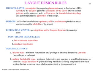
- 1. LAYOUT DESIGN RULES 21 PHYSICAL LAYER: prescription for preparing photomasks used in fabrication of ICs. Specify to the designer geometric constraints on the layout artwork so that patterns on the processed wafer will preserve the intended circuit topology and component/feature geometries of the design. PURPOSE: realize fabricated circuits optimum yield in smallest area possible without compromising the reliability of the circuit. DESIGN RULE WAIVER: any significant and/or frequent departure from design rules. TWO TYPES OF DESIGN RULES: a. line widths and separations b. interlayer registration DESIGN RULE SPECS: a. 'micron' rules - minimum feature sizes and spacings in absolute dimensions µm units (normal spec in industry) b. scalable 'lambda (λ)' rules - minimum feature sizes and spacings in scalable dimensions in terms of a single parameter λ (popularized by Mead and Conway and permits first order scaling; limited to narrow range of dimensions; tend to be conservative.) Kenneth R. Laker, University of Pennsylvania
- 2. 22 LAYOUT DESIGN RULES The Design Process can be Abstracted to Manageable Number of Layout Levels that Represent the Physical Features on the Processed Silicon Wafer, i.e. -> Two different substrates (i.e. original substrate + well or twin wells) -> Doped regions p- and n- transistor forming materials (e.g. sources and drains) -> Transistor gate electrodes -> Interconnect paths -> Interlayer contacts Kenneth R. Laker, University of Pennsylvania
- 3. CMOS N-WELL DESIGN RULES 23 wells at wells at A- N-WELL RULES same different COLOR LEGEND A1 = 10λ potential potential n-Well p-Well n+ A2 = 6λ A2 = 8λ Polysilicon p+ B- ACTIVE RULES B1 = 3λ Gate Oxide B4 = 3λ B3 = 5λ Field Oxide Metal 1 B2 = 3λ Metal 2 B6 = 3λ B5 = 5λ Metal 3 Contact/via C- POLY RULES C5 = 3λ C1 = 2λ C3 = 1λ C4 = 2λ C2 = 2λ Kenneth R. Laker, University of Pennsylvani
- 4. COLOR LEGEND E- CONTACT RULES E1 = 2λ E5 = 1λ E3 = 2λ 24 n-Well F2 = 3λ p-Well n+ F1 = 3λ Polysilicon E2 = 2λ E6 = 1λ E4 = 1λ F- METAL 1 p+ E7 = 1λ RULES Gate Oxide Field Oxide Metal 1 E8 = 3λ Metal 2 E9 = 6λ Metal 3 Contact/via J3 = 2λ E10 = 3λ I2 = 3λ G- VIA RULES J1 = 8λ I1 = 2λ G1 = 2λ G3 = 1λ J2 = 2λ H1 = 3λ J- METAL 2 J2 = 5λ RULES G4 = 1λ G2 = 3λ H2 = 4λ Kenneth R. Laker, University of Pennsylvania
- 5. EFFECT OF INSUFFICENT GATE EXTENSION 25 C- POLY RULE Violation! over-etched poly shrinks p+ drawn p+ region diffusion bloats p+ processed p+ region p+ p+ drawn poly region processed poly region source, drain short gate extension (C4) p+ p+ Kenneth R. Laker, University of Pennsylvania
- 6. 26 EFFECT OF INSUFFICENT SOURCE-DRAIN EXTENSION Another C- POLY RULE Violation! source diffusion mask is p+ poly mask is shifted left shifted right p+ drawn p+ region gate p+ processed p+ region drain drawn poly region processed poly region mask misalignment contact p+ changes length and/or width of device and sometimes completely eleminates it. Kenneth R. Laker, University of Pennsylvania
- 7. 27 TECHNOLOGY RELATED CAD ISSUES TWO BASIC CHECKS MUST BE COMPLETED TO ENSURE THE MASK DATBASE DEVELOPED IN LAYOUT CAN BE TURNED INTO A WORKING CHIP: a. To verify specified Design Rules have been obeyed (DESIGN RULE CHECK or DRC) b. To verify masks produce correct interconnected set of circuit elements (MASK CIRCUIT-EXTRACTION) Kenneth R. Laker, University of Pennsylvania
- 8. Functionality & performance specs 28 TYPICAL DESIGN FLOW FOR THE PRODUCTION Circuit topology or schematic OF AN IC MASK SET Initial sizing of transistors Estimate parasitic capacitances Stick diagram layout Mask layout design Design Rule Check (DRC) Resize & Circuit & parasitic extraction Modify Circuit simulation Improve Performance OK Layout Complete