1. International Journal of Computational Engineering Research||Vol, 03||Issue, 5||
www.ijceronline.com ||May ||2013|| Page 89
Pulsed Electrodeposition of Nano-Crystalline Ni with Uniform
Co-Depostion of Micron Sized Diamond Particles on Annealed
Copper Substrate
Prashant Kumar1
, Neelima Mahato2
, Vandana Singh2
, Raja Chaudhary2
,
Kantesh Balani2
1
Department of Metallurgical Engineering
Indian Institute of Technology, Banaras Hindu University, Varanasi- 221 005
2
Materials Science and Engineering, Indian Institute of Technology, Kanpur- 208 016
I. INTRODUCTION
In the current work, nanocrystalline Ni-Diamond films were synthesized by pulsed electrodeposition
using a watts bath . Depositions were optimized on the current density range of 50-200 mA/cm2
and
200mA/cm2
was best suitedto achieve a uniform equiaxed coating with a target of high Ni-Diamond content
owing to their superior corrosion resistance and enhanced hardness. Nowadays, in order to fabricate
nanocrystalline metallic films, many deposition techniques are available, such as sputtering, molecular beam
epitaxy, vacuum evaporation, sol-gel, thermal spray, etc. But all these methods require high precision process
control, which demand higher capital cost and incur huge material waste. But electrodeposition is an established
and inexpensive technology among other fabricating processes which is accomplished by fabricating metallic
alloys using low-temperature synthesis from aqueous solutions. This has an advantage of preparation of films
over a large surface area without impairing materials purity in a relatively shorter period of time. In the
electrodeposition process, the film properties mainly depend on deposition conditions, e.g, current density,
deposition potential, bath type density, deposition potential, bath type density, deposition potential, bath type the
electrochemical deposition conditions as well as physical parameters such as thickness, the substrate type, and
orientation, it is possible to control and optimize the electrodeposited films (such as coating thickness, cluster
size, etc.)
Nanosized Ni deposits require the application of much higher current densities, which normally leads to cracks
in films. Pulse electro deposition provides more uniform and crack-free deposits with required properties. The
ABSTRACT
Nanocrystalline nickel was deposited on annealed copper substrate of unit surface area (1
cm2
) via pulsed electrodeposition technique using potentiostat (model 263A, Princeton Applied
Research, USA) from Watts bath containing nickel sulfate, nickel chloride , boric acid and sodium
citrate. Diamond particles of three different dimensions, viz., 1, 3, and 6 micron were added
separately (5 g/L) to the watts bath and co-deposited along with nanocrystalline nickel.The
temperature was kept constant at 55 °C.The solution was sonicated for 45-60 minutes prior to
deposition to disperse the diamond particles uniformly in the bath. Depositions were carried out at
different current densities, viz., 50, 100 and 200 mA/ cm2
for different durations, i.e., 7, 14 and 21
minutes and best results are optimized for 200mA/cm2
so it is used for all process here .Scanning
electron micrographs(SEM) show uniform deposition of Microstructure of micron diamond on the
surface of copper embedded in the nickel matrix. Elemental mapping confirmed uniform deposition
of nickel and diamond with almost no cracks or pits. Mechanical properties such as, Vicker’s
hardness and wear properties were investigated using microindentation, tribology and laser
profilometry. Improved microstructural and mechanical properties were found in the case of
electrodeposited surfaces containing followed by 3 and 6 micron diamond. The properties were also
found better than those processed via stirring the solution during deposition.
KEYWORDS: Nanocrystalline Ni, Electrodeposition, Codeposition, Annealed copper.
2. Pulsed Electrodeposition Of Nano…
www.ijceronline.com ||May ||2013|| Page 90
pulse electrodeposited Nano crystalline (nc) Ni-Diamond films can receive great attention due to enhanced
mechanical properties, and improved corrosion resistance when the Nanocrystalline films are dense and defect
free.
1.1.PROBLEM STATEMENT REGARDING EXPERIMENT –Major obstacle regarding the experimental
research was that we were unable to get a uniform co- deposition of the diamond particles on the annealed
copper substrate (due to very early settling down of diamond particles owing to their higher density) during the
pulsed electro deposition of nickel on the annealed Cu substrate using potentiostat and hence we cannot get
effective simultaneous deposition of both Ni and diamond.
1.2.STRATEGY USED TO OVERCOME- We used a ultrasonicator during the pulsed deposition which
sent ultrasonic waves into solution and woúld not allow the diamond particls to settle down and we can
get an uniform coating with uniform deposition of diamond particles.
II. EXPERIMENTAL DETAILS
Nano crystalline nickel was deposited on annealed copper substrate of unit surface area (1 cm2
) via
pulsed electro deposition technique using potentiostat (model 263A, Princeton Applied Research, USA) from
Watts bath containing nickel (NiSO47H2O), nickel chloride (NiCl2.6H2O), boric acid and citrate complexing
agentsodium citrate( Na3C6H5O7.2H2O). Diamond particles of three different dimensions, viz., 1, 3, and 6
micron were added separately (5 g/L) to the watts bath and co-deposited along with Nano crystalline nickel.The
temperature was kept constant at 55 °C. The solution was sonicated for 45-60 minutes prior to deposition to
disperse the diamond particles uniformly the bath.
Electrolyte Bath Compositions Utilized for the Co-deposition of Ni-Diamond film
Composition Concentration Parameters
NiSO4.7H2O, g/L - 250
NiCl2.6H2O,g/L - 40 Temp. = at 55 °C
H3BO3, g/L - 40
Sodium citrate, g/L - 25
Depositions were carried out at different current densities, viz., in 50, 100 and 200 mA/ cm2
for different
durations, i.e., 7, 14 and 21 minutes. One cycle of deposition corresponds to 1 minute. Scanning electron
micrographs show uniform deposition of Microstructure of micron diamond on the surface of copper embedded
in the nickel matrix. Elemental mapping confirmed uniform deposition of nickel and diamond with almost no
cracks or pits. The analysis of the electrodeposited surfaces were done using SEM, and micromechanical
properties, such as, Vicker’s hardness . Improved microstructural and mechanical properties were found in the
case of electrodeposited surfaces containing 6 micron diamond followed by 3 and 1 micron diamond. The
mechanical properties were also found better than those processed via stirring the solution during deposition.
2.1.POTENTIOSTAT USED FOR PULSED ELECTRODEPOSITION :- (MODEL 263A, PRINCETON
APPLIED RESEARCH, USA)
3. Pulsed Electrodeposition Of Nano…
www.ijceronline.com ||May ||2013|| Page 91
OBSERVATIONS AND RESULTS –
Experimental parameter I –3 micron diamond, (5 g/L), 60 ml solution , 30 min prior to sonication , 3
min deposition + 3 min sonication , Temperature 50-55 degree Celsius
21 cycles intermittent (electrodes kept dipped while sonication intervals) no deposition while
sonication
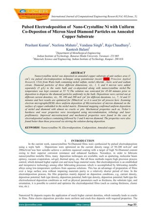
THE Images on the
right hand side are
the S.E.M images of
the equiaxed
NANOCRYSTALL-
INE DEPOSITED
NICKEL( with
uniformly
deposited 3
MICRON DIAMOND
OVER IT) on the
annealed Cu
substrate
ABOVE SHOWN IS THE ELEMENTAL MAPPING which shows two spectrums viz: SPECTRUM 1 and
SOECTRUM 2
From elemental mapping we can clearly see that the CARBON WEIGHT % at SPECTRUM 2 is very high
around 80 % and presence of very low Ni % which indicates and proves the presence of diamond particle
over there
4. Pulsed Electrodeposition Of Nano…
www.ijceronline.com ||May ||2013|| Page 92
S.E.M Image Of The Uniformly Deposited Equiaxed NANOCRYSTALLINE Ni( With 6 MICRON
DIAMOND PARTICLES) EMBEDDED OVER IT ) On The Cu Substrate At Different Magnifications Of
10 Micron And 1 Micron
Experimental parameter III - 1 MICRON DIAMOND 21 CYCLES
DEPOSITION
S.E.M image of the
uniformly deposited
equiaxed nano
crystalline Ni( with 1
MICRON DIAMOND
PARTICLES) EMBEDDED
OVER IT ) on the
annealed Cu substrate
at magnification 2
micron
5. Pulsed Electrodeposition Of Nano…
www.ijceronline.com ||May ||2013|| Page 93
III.
ANNEALED
COPPER SAMPLE
NI- 1 MICRON
DIAMOND
COATING
21 CYCLES
NI- 3 MICRON
DIAMOND COATING
21 CYCLES
NI- 6 MICRON DIAMOND
COATING
21 CYCLES
108.5 433.8 469.8 481.7
108.3 435.6 475.2 485.6
112.6 439.2 468.5 489.6
109.7 439.6 472.5 488.6
111.8 443.3 478.1 489.3
AVERAGE =110.18 AVERAGE =438.3 AVERAGE = 472.82 AVERAGE = 486.96
VARIATION IN THE VALUE OF VICKERS HARDNESS OF THE ANNEALED COPPER
SAMPLE ON THE ELECTRODEPOSITION OF NANOCRYSTALLINE NICKEL
EMBEDDED WITH MICRON SIZED DIAMOND
MEASURMENT OF VICKERS HARDNESS OF THE SAMPLES -
6. Pulsed Electrodeposition Of Nano…
www.ijceronline.com ||May ||2013|| Page 94
III. CONCLUSION
The enhanced content of nanocrystalline Ni with increased current density of around 200 mA/cm2
allows achieving enhanced hardness in comparison to that of low Ni deposits. Tremendous increase in the
value of Vickers hardness of the annealed copper substrate is noticed on the electrodeposition of
nanocrystalline film of Ni coated with micron sized diamond particles . The best result of the increased values of
hardness was found with 6 micron diamond embedded nanocrystalline Ni film on the annealed copper sample
.So Superior Ni-Diamond coatings, with improved corrosion resistance and hardness, can been developed on an
annealed copper substrate These coatings can be used in single and multilayer electronic packaging, enhancing
mechanical properties of surfaces, mining, and ship building However, it is important to note that superior
corrosion resistance can only be possible when the nanocrystalline films are dense and defect free.
REFERENCES
[1] V.P. Glibin, B.V. Kuznetsov, and T.N. Vorobyova, J.
[2] Alloys & Compounds, 386 (2005),
[3] E. Pellicer et al., Proc. in the International Conference
[4] on Advanced Materials (Zurich: IRIS, 2009),
[5] H. Natter and R. Hempelmann, Electrochemica
[6] Acta, 49 (2003),
[7] M. Troyon and L. Wang, Appl. Surf. Sci., 103 (1996),
[8] T. Miyake et al., Thin Solid Films, 397 (2001),
[9] I. Baskaran et al., Mater. Lett.,60 (2006), pp. 1990–
[10] 1995.
[11] X. Chui and W. Chen, J. Electrochemical Society,