Genislab builds better products and faster go-to-market with Lean project man...
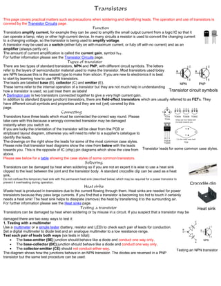
Transistors
1. Transistors
This page covers practical matters such as precautions when soldering and identifying leads. The operation and use of transistors is
covered by the Transistor Circuits page.
Function
Transistors amplify current, for example they can be used to amplify the small output current from a logic IC so that it
can operate a lamp, relay or other high current device. In many circuits a resistor is used to convert the changing current
to a changing voltage, so the transistor is being used to amplify voltage.
A transistor may be used as a switch (either fully on with maximum current, or fully off with no current) and as an
amplifier (always partly on).
The amount of current amplification is called the current gain, symbol hFE.
For further information please see the Transistor Circuits page.
Types of transistor
There are two types of standard transistors, NPN and PNP, with different circuit symbols. The letters
refer to the layers of semiconductor material used to make the transistor. Most transistors used today
are NPN because this is the easiest type to make from silicon. If you are new to electronics it is best
to start by learning how to use NPN transistors.
The leads are labelled base (B), collector (C) and emitter (E).
These terms refer to the internal operation of a transistor but they are not much help in understanding
how a transistor is used, so just treat them as labels!
A Darlington pair is two transistors connected together to give a very high current gain.
In addition to standard (bipolar junction) transistors, there are field-effect transistors which are usually referred to as FETs. They
have different circuit symbols and properties and they are not (yet) covered by this
page.
Connecting
Transistors have three leads which must be connected the correct way round. Please
take care with this because a wrongly connected transistor may be damaged
instantly when you switch on.
If you are lucky the orientation of the transistor will be clear from the PCB or
stripboard layout diagram, otherwise you will need to refer to a supplier's catalogue to
identify the leads.
The drawings on the right show the leads for some of the most common case styles.
Please note that transistor lead diagrams show the view from below with the leads
towards you. This is the opposite of IC (chip) pin diagrams which show the view from
above.
Please see below for a table showing the case styles of some common transistors.
Soldering
Transistors can be damaged by heat when soldering so if you are not an expert it is wise to use a heat sink
clipped to the lead between the joint and the transistor body. A standard crocodile clip can be used as a heat
sink.
Do not confuse this temporary heat sink with the permanent heat sink (described below) which may be required for a power transistor to
prevent it overheating during operation.
Heat sinks
Waste heat is produced in transistors due to the current flowing through them. Heat sinks are needed for power
transistors because they pass large currents. If you find that a transistor is becoming too hot to touch it certainly
needs a heat sink! The heat sink helps to dissipate (remove) the heat by transferring it to the surrounding air.
For further information please see the Heat sinks page.
Testing a transistor
Transistors can be damaged by heat when soldering or by misuse in a circuit. If you suspect that a transistor may be
damaged there are two easy ways to test it:
1. Testing with a multimeter
Use a multimeter or a simple tester (battery, resistor and LED) to check each pair of leads for conduction.
Set a digital multimeter to diode test and an analogue multimeter to a low resistance range.
Test each pair of leads both ways (six tests in total):
The base-emitter (BE) junction should behave like a diode and conduct one way only.
The base-collector (BC) junction should behave like a diode and conduct one way only.
The collector-emitter (CE) should not conduct either way.
The diagram shows how the junctions behave in an NPN transistor. The diodes are reversed in a PNP
transistor but the same test procedure can be used.
Transistor circuit symbols
Transistor leads for some common case styles.
Crocodile clip
Heat sink
Testing an NPN transistor
2. 2. Testing in a simple switching circuit
Connect the transistor into the circuit shown on the right which uses the transistor as a switch. The supply
voltage is not critical, anything between 5 and 12V is suitable. This circuit can be quickly built on
breadboard for example. Take care to include the 10k resistor in the base connection or you will destroy
the transistor as you test it!
If the transistor is OK the LED should light when the switch is pressed and not light when the switch is
released.
To test a PNP transistor use the same circuit but reverse the LED and the supply voltage.
Some multimeters have a 'transistor test' function which provides a known base current and measures the
collector current so as to display the transistor's DC current gain hFE.
Transistor codes
There are three main series of transistor codes used in the UK:
Codes beginning with B (or A), for example BC108, BC478
The first letter B is for silicon, A is for germanium (rarely used now). The second letter indicates the type; for example C
means low power audio frequency; D means high power audio frequency; F means low power high frequency. The rest of the
code identifies the particular transistor. There is no obvious logic to the numbering system. Sometimes a letter is added to the
end (eg BC108C) to identify a special version of the main type, for example a higher current gain or a different case style. If a
project specifies a higher gain version (BC108C) it must be used, but if the general code is given (BC108) any transistor with
that code is suitable.
Codes beginning with TIP, for example TIP31A
TIP refers to the manufacturer: Texas Instruments Power transistor. The letter at the end identifies versions with different
voltage ratings.
Codes beginning with 2N, for example 2N3053
The initial '2N' identifies the part as a transistor and the rest of the code identifies the particular transistor. There is no obvious
logic to the numbering system.
Choosing a transistor
Most projects will specify a particular transistor, but if necessary you can usually substitute an equivalent transistor from the wide
range available. The most important properties to look for are the maximum collector current IC and the current gain hFE. To make
selection easier most suppliers group their transistors in categories determined either by their typical use or maximum power rating.
To make a final choice you will need to consult the tables of technical data which are normally provided in catalogues. They contain a
great deal of useful information but they can be difficult to understand if you are not familiar with the abbreviations used. The table
below shows the most important technical data for some popular transistors, tables in catalogues and reference books will usually
show additional information but this is unlikely to be useful unless you are experienced. The quantities shown in the table are
explained below.
NPN transistors
Code Structure
Case
style
IC
max.
VCE
max.
hFE
min.
Ptot
max.
Category
(typical use)
Possible
substitutes
BC107 NPN TO18 100mA 45V 110 300mW Audio, low power BC182 BC547
BC108 NPN TO18 100mA 20V 110 300mW General purpose, low power
BC108C
BC183 BC548
BC108C NPN TO18 100mA 20V 420 600mW General purpose, low power
BC109 NPN TO18 200mA 20V 200 300mW Audio (low noise), low power BC184 BC549
BC182 NPN TO92C 100mA 50V 100 350mW General purpose, low power
BC107
BC182L
BC182L NPN TO92A 100mA 50V 100 350mW General purpose, low power BC107 BC182
BC547B NPN TO92C 100mA 45V 200 500mW Audio, low power BC107B
BC548B NPN TO92C 100mA 30V 220 500mW General purpose, low power BC108B
BC549B NPN TO92C 100mA 30V 240 625mW Audio (low noise), low power BC109
2N3053 NPN TO39 700mA 40V 50 500mW General purpose, low power BFY51
BFY51 NPN TO39 1A 30V 40 800mW General purpose, medium power BC639
BC639 NPN TO92A 1A 80V 40 800mW General purpose, medium power BFY51
TIP29A NPN TO220 1A 60V 40 30W General purpose, high power
TIP31A NPN TO220 3A 60V 10 40W General purpose, high power
TIP31C
TIP41A
TIP31C NPN TO220 3A 100V 10 40W General purpose, high power
TIP31A
TIP41A
TIP41A NPN TO220 6A 60V 15 65W General purpose, high power
2N3055 NPN TO3 15A 60V 20 117W General purpose, high power
Please note: the data in this table was compiled from several sources which are not entirely consistent! Most of the discrepancies are minor, but please consult
information from your supplier if you require precise data.
PNP transistors
A simple switching circuit
to test an NPN transistor
3. Code Structure
Case
style
IC
max.
VCE
max.
hFE
min.
Ptot
max.
Category
(typical use)
Possible
substitutes
BC177 PNP TO18 100mA 45V 125 300mW Audio, low power BC477
BC178 PNP TO18 200mA 25V 120 600mW General purpose, low power BC478
BC179 PNP TO18 200mA 20V 180 600mW Audio (low noise), low power
BC477 PNP TO18 150mA 80V 125 360mW Audio, low power BC177
BC478 PNP TO18 150mA 40V 125 360mW General purpose, low power BC178
TIP32A PNP TO220 3A 60V 25 40W General purpose, high power TIP32C
TIP32C PNP TO220 3A 100V 10 40W General purpose, high power TIP32A
Please note: the data in this table was compiled from several sources which are not entirely consistent! Most of the discrepancies are minor, but please consult
information from your supplier if you require precise data.
Structure This shows the type of transistor, NPN or PNP. The polarities of the two types are different, so if you are
looking for a substitute it must be the same type.
Case style There is a diagram showing the leads for some of the most common case styles in the Connecting section
above. This information is also available in suppliers' catalogues.
IC max. Maximum collector current.
VCE max. Maximum voltage across the collector-emitter junction.
You can ignore this rating in low voltage circuits.
hFE This is the current gain (strictly the DC current gain). The guaranteed minimum value is given because the
actual value varies from transistor to transistor - even for those of the same type! Note that current gain is just
a number so it has no units.
The gain is often quoted at a particular collector current IC which is usually in the middle of the transistor's
range, for example '100@20mA' means the gain is at least 100 at 20mA. Sometimes minimum and maximum
values are given. Since the gain is roughly constant for various currents but it varies from transistor to
transistor this detail is only really of interest to experts.
Why hFE? It is one of a whole series of parameters for transistors, each with their own symbol. There are too
many to explain here.
Ptot max. Maximum total power which can be developed in the transistor, note that a heat sink will be required to
achieve the maximum rating. This rating is important for transistors operating as amplifiers, the power is
roughly IC × VCE. For transistors operating as switches the maximum collector current (IC max.) is more
important.
Category This shows the typical use for the transistor, it is a good starting point when looking for a substitute.
Catalogues may have separate tables for different categories.
Possible substitutes These are transistors with similar electrical properties which will be suitable substitutes in most circuits.
However, they may have a different case style so you will need to take care when placing them on the circuit
board.
Darlington pair
This is two transistors connected together so that the amplified current from the first is amplified further by the
second transistor. This gives the Darlington pair a very high current gain such as 10000. Darlington pairs are
sold as complete packages containing the two transistors. They have three leads (B, C and E) which are
equivalent to the leads of a standard individual transistor.
You can make up your own Darlington pair from two transistors.
For example:
For TR1 use BC548B with hFE1 = 220.
For TR2 use BC639 with hFE2 = 40.
The overall gain of this pair is hFE1 × hFE2 = 220 × 40 = 8800.
The pair's maximum collector current IC(max) is the same as TR2.
Transistor Circuits
This page explains the operation of transistors in circuits. Practical matters such as testing, precautions when soldering and identifying
leads are covered by the Transistors page.
Types
4. There are two types of standard transistors, NPN and PNP, with different circuit symbols. The letters
refer to the layers of semiconductor material used to make the transistor. Most transistors used today
are NPN because this is the easiest type to make from silicon. This page is mostly about NPN
transistors and if you are new to electronics it is best to start by learning how to use these first.
The leads are labelled base (B), collector (C) and emitter (E).
These terms refer to the internal operation of a transistor but they are not much help in understanding
how a transistor is used, so just treat them as labels!
A Darlington pair is two transistors connected together to give a very high current gain.
In addition to standard (bipolar junction) transistors, there are field-effect transistors which are usually referred to as FETs. They
have different circuit symbols and properties and they are not (yet) covered by this page. Transistor
currents
The diagram shows the two current paths through a transistor. You can build this circuit with two standard
5mm red LEDs and any general purpose low power NPN transistor (BC108, BC182 or BC548 for example).
The small base current controls the larger collector current.
When the switch is closed a small current flows into the base (B) of the transistor. It is just enough to
make LED B glow dimly. The transistor amplifies this small current to allow a larger current to flow through
from its collector (C) to its emitter (E). This collector current is large enough to make LED C light brightly.
When the switch is open no base current flows, so the transistor switches off the collector current. Both
LEDs are off.
A transistor amplifies current and can be used as a switch.
This arrangement where the emitter (E) is in the controlling circuit (base current) and in the controlled circuit
(collector current) is called common emitter mode. It is the most widely used arrangement for transistors
so it is the one to learn first.
Functional model of an NPN transistor
The operation of a transistor is difficult to explain and understand in terms of its internal structure. It is more
helpful to use this functional model:
The base-emitter junction behaves like a diode.
A base current IB flows only when the voltage VBE across the base-emitter junction is 0.7V or more.
The small base current IB controls the large collector current Ic.
Ic = hFE × IB (unless the transistor is full on and saturated)
hFE is the current gain (strictly the DC current gain), a typical value for hFE is 100 (it has no units because
it is a ratio)
The collector-emitter resistance RCE is controlled by the base current IB:
o IB = 0 RCE = infinity transistor off
o IB small RCE reduced transistor partly on
o IB increased RCE = 0 transistor full on ('saturated')
Additional notes:
A resistor is often needed in series with the base connection to limit the base current IB and prevent the
transistor being damaged.
Transistors have a maximum collector current Ic rating.
The current gain hFE can vary widely, even for transistors of the same type!
A transistor that is full on (with RCE = 0) is said to be 'saturated'.
When a transistor is saturated the collector-emitter voltage VCE is reduced to almost 0V.
When a transistor is saturated the collector current Ic is determined by the supply voltage and the external resistance in the
collector circuit, not by the transistor's current gain. As a result the ratio Ic/IB for a saturated transistor is less than the current
gain hFE.
The emitter current IE = Ic + IB, but Ic is much larger than IB, so roughly IE = Ic.
There is a table showing technical data for some popular transistors on the transistors page.
Darlington pair
This is two transistors connected together so that the current amplified by the first is amplified further
by the second transistor. The overall current gain is equal to the two individual gains multiplied
together:
Darlington pair current gain, hFE = hFE1 × hFE2
(hFE1 and hFE2 are the gains of the individual transistors)
This gives the Darlington pair a very high current gain, such as 10000, so that only a tiny base current
is required to make the pair switch on.
A Darlington pair behaves like a single transistor with a very high current gain. It has three leads
(B, C and E) which are equivalent to the leads of a standard individual transistor. To turn on there must be 0.7V
across both the base-emitter junctions which are connected in series inside the Darlington pair, therefore it
requires 1.4V to turn on.
Darlington pairs are available as complete packages but you can make up your own from two transistors; TR1
can be a low power type, but normally TR2 will need to be high power. The maximum collector current Ic(max) for the pair is the same
as Ic(max) for TR2.
Transistor circuit symbols
5. A Darlington pair is sufficiently sensitive to respond to the small current passed by your skin and it can be used to make a touch-
switch as shown in the diagram. For this circuit which just lights an LED the two transistors can be any general purpose low power
transistors. The 100k resistor protects the transistors if the contacts are linked with a piece of wire.
Using a transistor as a switch
When a transistor is used as a switch it must be either OFF or fully ON. In the fully ON state the voltage VCE
across the transistor is almost zero and the transistor is said to be saturated because it cannot pass any more
collector current Ic. The output device switched by the transistor is usually called the 'load'.
The power developed in a switching transistor is very small:
In the OFF state: power = Ic × VCE, but Ic = 0, so the power is zero.
In the full ON state: power = Ic × VCE, but VCE = 0 (almost), so the power is very small.
This means that the transistor should not become hot in use and you do not need to consider its maximum
power rating. The important ratings in switching circuits are the maximum collector current Ic(max) and the minimum current gain
hFE(min). The transistor's voltage ratings may be ignored unless you are using a supply voltage of more than about 15V. There is a
table showing technical data for some popular transistors on the transistors page.
For information about the operation of a transistor please see the functional model above.
Protection diode
If the load is a motor, relay or solenoid (or any other device with a coil) a diode must be connected
across the load to protect the transistor from the brief high voltage produced when the load is switched
off. The diagram shows how a protection diode is connected 'backwards' across the load, in this case
a relay coil.
Current flowing through a coil creates a magnetic field which collapses suddenly when the current is
switched off. The sudden collapse of the magnetic field induces a brief high voltage across the coil
which is very likely to damage transistors and ICs. The protection diode allows the induced voltage to
drive a brief current through the coil (and diode) so the magnetic field dies away quickly rather than
instantly. This prevents the induced voltage becoming high enough to cause damage to transistors and ICs.
When to use a relay
Transistors cannot switch AC or high voltages (such as mains electricity) and they are not usually a good choice for
switching large currents (> 5A). In these cases a relay will be needed, but note that a low power transistor may still be
needed to switch the current for the relay's coil!
Advantages of relays:
Relays can switch AC and DC, transistors can only switch DC.
Relays can switch high voltages, transistors cannot.
Relays are a better choice for switching large currents (> 5A).
Relays can switch many contacts at once.
Disadvantages of relays:
Relays are bulkier than transistors for switching small currents.
Relays cannot switch rapidly, transistors can switch many times per second.
Relays use more power due to the current flowing through their coil.
Relays require more current than many ICs can provide, so a low power transistor may be needed to
switch the current for the relay's coil.
Connecting a transistor to the output from an IC
Most ICs cannot supply large output currents so it may be necessary to use a transistor to switch the larger current required for output
devices such as lamps, motors and relays. The 555 timer IC is unusual because it can supply a relatively large current of up to 200mA
which is sufficient for some output devices such as low current lamps, buzzers and many relay coils without needing to use a
transistor.
A transistor can also be used to enable an IC connected to a low voltage supply (such as 5V) to switch the current for an output
device with a separate higher voltage supply (such as 12V). The two power supplies must be linked, normally this is done by linking
their 0V connections. In this case you should use an NPN transistor.
A resistor RB is required to limit the current flowing into the base of the transistor and prevent it
being damaged. However, RB must be sufficiently low to ensure that the transistor is thoroughly
saturated to prevent it overheating, this is particularly important if the transistor is switching a
large current (> 100mA). A safe rule is to make the base current IB about five times larger than
the value which should just saturate the transistor.
Choosing a suitable NPN transistor
The circuit diagram shows how to connect an NPN transistor, this will switch
on the load when the IC output is high. If you need the opposite action, with
the load switched on when the IC output is low (0V) please see the circuit for a
PNP transistor below.
The procedure below explains how to choose a suitable switching transistor.
1. The transistor's maximum collector current Ic(max) must be greater than the load
current Ic.
load current Ic =
supply voltage Vs
load resistance RL
Relays
6. 2. The transistor's minimum current gain hFE(min) must be at least five times the load current Ic divided by the maximum output
current from the IC.
hFE(min) > 5 ×
load current Ic
max. IC current
3. Choose a transistor which meets these requirements and make a note of its properties: Ic(max) and hFE(min).
There is a table showing technical data for some popular transistors on the transistors page.
4. Calculate an approximate value for the base resistor:
RB =
Vc × hFE where Vc = IC supply voltage
(in a simple circuit with one supply this is Vs)5 × Ic
5. For a simple circuit where the IC and the load share the same power supply (Vc = Vs) you may prefer to use: RB = 0.2 × RL × hFE
6. Then choose the nearest standard value for the base resistor.
7. Finally, remember that if the load is a motor or relay coil a protection diode is required.
Example:
The output from a 4000 series CMOS IC is required to operate a relay with a 100 coil.
The supply voltage is 6V for both the IC and load. The IC can supply a maximum current of 5mA.
1. Load current = Vs/RL = 6/100 = 0.06A = 60mA, so transistor must have Ic(max) > 60mA.
2. The maximum current from the IC is 5mA, so transistor must have hFE(min) > 60 (5 × 60mA/5mA).
3. Choose general purpose low power transistor BC182 with Ic(max) = 100mA and hFE(min) = 100.
4. RB = 0.2 × RL × hFE = 0.2 × 100 × 100 = 2000 . so choose RB = 1k8 or 2k2.
5. The relay coil requires a protection diode.
Choosing a suitable PNP transistor
The circuit diagram shows how to connect a PNP transistor, this will switch on the load when the IC
output is low (0V). If you need the opposite action, with the load switched on when the IC output is
high please see the circuit for an NPN transistor above.
The procedure for choosing a suitable PNP transistor is exactly the same as that for an NPN
transistor described above.
Using a transistor switch with sensors
The top circuit diagram shows an LDR (light sensor) connected
so that the LED lights when the LDR is in darkness. The
variable resistor adjusts the brightness at which the transistor
switches on and off. Any general purpose low power transistor can
be used in this circuit.
The 10k fixed resistor protects the transistor from excessive base current (which will destroy
it) when the variable resistor is reduced to zero. To make this circuit switch at a suitable
brightness you may need to experiment with different values for the fixed resistor, but it must not
be less than 1k .
If the transistor is switching a load with a coil, such as a motor or relay, remember to add a
protection diode across the load.
The switching action can be inverted, so the LED lights when the LDR is brightly lit, by
swapping the LDR and variable resistor. In this case the fixed resistor can be omitted because the LDR resistance cannot be reduced
to zero.
Note that the switching action of this circuit is not particularly good because there will be an intermediate brightness when the
transistor will be partly on (not saturated). In this state the transistor is in danger of overheating unless it is switching a small current.
There is no problem with the small LED current, but the larger current for a lamp, motor or relay is likely to cause overheating.
Other sensors, such as a thermistor, can be used with this circuit, but they may require a different variable resistor. You can calculate
an approximate value for the variable resistor (Rv) by using a multimeter to find the minimum and maximum values of the sensor's
resistance (Rmin and Rmax):
Variable resistor, Rv = square root of (Rmin × Rmax)
For example an LDR: Rmin = 100 , Rmax = 1M , so Rv = square root of (100 × 1M) = 10k .
You can make a much better switching circuit with sensors connected to a suitable IC (chip). The switching action will be much
sharper with no partly on state.
A transistor inverter (NOT gate)
Inverters (NOT gates) are available on logic ICs but if you only require one inverter it is usually better
to use this circuit. The output signal (voltage) is the inverse of the input signal:
When the input is high (+Vs) the output is low (0V).
When the input is low (0V) the output is high (+Vs).
Any general purpose low power NPN transistor can be used. For general use RB = 10k and RC = 1k
, then the inverter output can be connected to a device with an input impedance (resistance) of at
least 10k such as a logic IC or a 555 timer (trigger and reset inputs).
If you are connecting the inverter to a CMOS logic IC input (very high impedance) you can increase RB
to 100k and RC to 10k , this will reduce the current used by the inverter.