
Recommended
More Related Content
What's hot
What's hot (20)
Viewers also liked
Viewers also liked (15)
Similar to Types of PCB Designing Layers
Similar to Types of PCB Designing Layers (20)
Recently uploaded
Recently uploaded (20)
Types of PCB Designing Layers
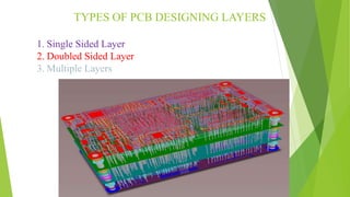
- 1. TYPES OF PCB DESIGNING LAYERS 1. Single Sided Layer 2. Doubled Sided Layer 3. Multiple Layers
- 2. SINGLE SIDED CIRCUIT BOARDS Single Sided PCB Single Sided Layer
- 3. Also it is start point of the invention, it still plays a major role in the industry. This Single Sided PCB is invented to give a good mechanical base for components. Reliability of connections compared to hand wiring and another big benefit is ease of assembly production of an electronic device in volume. In through hole device technology, it does have it’s limitations in interconnecting large numbers of components as all the tracks are on one side. Due to surface finishes like Lead free hot air level, Nickel Gold and organic surface protection, single sided boards can used for surface mount devices as well as through hole.
- 4. Procedure For Making Single Sided Layer Board
- 5. Doubled Sided Circuit Boards Double Sided PCB Double Sided Layer
- 6. The double sided “PTH” (plated through holes) PCB is the universal workhorse of the electronics industry. Increasing complexity and density of components. In this “Plated Through Holes” where the copper connections go right through the connecting holes to the opposite side of the board. This PTH Connections either form simple electrical connection between both sides of the PCB (Via Holes),or electrical connectivity and mechanical support for leaded components.
- 7. Procedure For Making Doubled Sided Layer Board
- 8. Multiple Layer Circuit Board Multiple Layer PCB Multiple Layers
- 9. The multilayer PCB is the development of the double sided PCB. Increasing complexity and density of components. Adding just a power and ground plane to the inside of the board allowed the components to be powered with just two plated holes to the inner layers rather than a track back to a power/ground point. Highly complex and compact circuits. High Density and Hole Technology.
- 10. Procedure For Making Doubled Sided Layer Board
- 11. Thank you